EasyManua.ls Logo

Quectel FC80A - Functional Diagram; Evaluation Board; Application Interfaces; Pin Assignment

Quectel FC80A
52 pages
To Next Page IconTo Next Page
To Previous Page IconTo Previous Page
Loading...
Wi-Fi&Bluetooth Module Series
FC80A_Hardware_Design 12 / 43
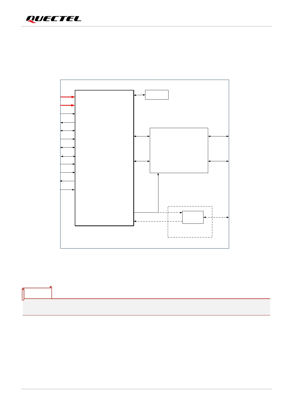
2.3. Functional Diagram
The following figure shows a block diagram of FC80A.
Main Chip
ANT_WIFI1
ANT_WIFI0/BT
37.4 MHz
XO
Switch/
BT xLNA
ANT_BT
Optional dedicated BT
antenna switch/xLNA
VDDIO
VBAT
WLAN_WAKE
SDIO_VSEL
BT_EN
BT UART
PCM
WLAN_EN
SDIO 3.0
WLAN_SLP_CLK
HOST_WAKE_BT
BT_WAKE_HOST
TX/RX
Blocks
Figure 1: Functional Diagram of FC80A
2.4. Evaluation Board
To help customers to develop applications with FC80A, Quectel supplies an evaluation board
(UMTS&LTE EVB), an RS-232 to USB converter cable, a USB data cable, a power adapter, antennas
and other peripherals to control or test the module. For details, see document [1].
Dedicated Bluetooth antenna (ANT_BT) is optional according to the order code of the module.
NOTE

Related product manuals