Do you have a question about the Quectel EG91-NAXD and is the answer not in the manual?
Details FCC certification requirements and conditions for mobile devices.
Provides safety precautions for operating, service, and repair of EG91 series modules.
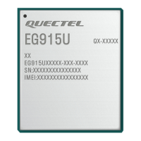
Overview of EG91 series module, its variants, and frequency bands supported.
Details the key features of the EG91 series module, including power supply and transmitting power.
Presents a block diagram of the EG91 series module illustrating its major functional parts.
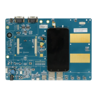
Describes the evaluation tools provided by Quectel for EG91 series module testing.
Describes the EG91 series module's pads and sub-interfaces like power, SIM, USB, UART.
Illustrates the pin assignment of the EG91 series module with a top view diagram.
Details the pin definition and description of EG91 series module pins.
Briefly outlines the operating modes of the EG91 series module.
Explains how EG91 series module reduces current consumption during sleep mode.
Describes power supply pins, ratings, voltage drop, and reference designs.
Details how to turn on/off the module using PWRKEY or AT commands.
Describes how to reset the EG91 module using the RESET_N pin and its reference circuit.
Details the two (U)SIM interfaces and their support for 1.8V and 3.0V SIM cards.
Covers the integrated USB interface, its specifications, and pin definition.
Describes the two UART interfaces (main and debug) and their features.
Explains the PCM digital interface for audio and the I2C interface.
Details the SPI interface, acting as master only, for communication with peripherals.
Describes the NETLIGHT pin for network status indication and its logic level changes.
Explains the STATUS pin as an operation status indicator for the module.
Details the ADC interface and how to read voltage values on the ADC0 pin.
Describes the behavior of the RI pin and how it can be configured.
Explains the USB_BOOT pin for entering emergency download mode for firmware upgrade.
Introduces the integrated GNSS solution supporting GPS, GLONASS, BeiDou, Galileo, QZSS.
Presents GNSS performance metrics like sensitivity and TTFF.
Provides layout guidelines for optimal GNSS antenna and circuit design.
Details the pin definition and operating frequencies for main and Rx-diversity antennas.
Shows a reference design for ANT_MAIN and ANT_DIV antenna pads with matching circuits.
Provides reference designs for microstrip and coplanar waveguide RF layout.
Details the pin definition and frequency specification for the GNSS antenna interface.
Lists requirements and recommends connectors for antenna installation.
Lists the absolute maximum ratings for power supply and voltage on module pins.
Details the power supply ratings for VBAT_BB and VBAT_RF pins.
Specifies the operation, extended, and storage temperature ranges for the module.
Presents current consumption values for EG91 series modules across various states.
Shows conducted RF receiving sensitivity for EG91 series modules across frequencies.
Details the module's electrostatic discharge characteristics and handling precautions.
Provides principles for thermal consideration and heatsink design for optimal performance.
Describes the mechanical dimensions of the EG91 module, including top and side views.
Provides the recommended footprint for the EG91 series module on the PCB.
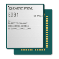
Shows the top and bottom views of the EG91 module for identification.
Details storage requirements, conditions, and floor life for the module.
Covers manufacturing processes like solder paste application and recommended reflow profiles.
Describes the vacuum-sealed bag packaging, reel dimensions, and tape details.
| Brand | Quectel |
|---|---|
| Model | EG91-NAXD |
| Category | Control Unit |
| Language | English |