Raisecom
ISCOM5508-GP (A) Hardware Description
Raisecom Proprietary and Confidential
Copyright © Raisecom Technology Co., Ltd.
7
Figures
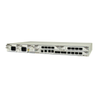
Figure 1-1 Appearance of the ISCOM5508-GP chassis ......................................................................................... 2
Figure 1-2 Distribution of slots on the ISCOM5508-GP ....................................................................................... 2
Figure 2-1 Appearance of the main control switching card (GPSC) ...................................................................... 5
Figure 2-2 Appearance of the GP4A subcard ......................................................................................................... 5
Figure 2-3 Appearance of the GE4B subcard ......................................................................................................... 6
Figure 2-4 Appearance of the WDFA4 subcard ..................................................................................................... 6
Figure 2-5 Appearance of the power module ......................................................................................................... 6
Figure 2-6 Appearance of the fan module .............................................................................................................. 7
Figure 2-7 Hardware information label on the ISCOM5508-GP ........................................................................... 7
Figure 2-8 Panel of the GPSC card ........................................................................................................................ 8
Figure 2-9 Panel of the GP4A subcard ................................................................................................................. 11
Figure 2-10 Panel of the GE4B subcard ............................................................................................................... 13
Figure 2-11 Panel of the WDFA4 subcard ........................................................................................................... 14
Figure 2-12 Panel of the RPA1101 power module ............................................................................................... 18
Figure 2-13 Panel of the RPD1101 power module ............................................................................................... 19
Figure 2-14 Panel of the FANS306 module ......................................................................................................... 21
Figure 3-1 LC/PC fiber connector ........................................................................................................................ 25
Figure 3-2 SC/PC fiber connector ........................................................................................................................ 25
Figure 3-3 FC/PC fiber connector ........................................................................................................................ 26
Figure 3-4 Ethernet cable ..................................................................................................................................... 27
Figure 3-5 Straight-through cable wiring ............................................................................................................. 28
Figure 3-6 Crossover cable wiring ....................................................................................................................... 29
Figure 3-7 Configuration cable ............................................................................................................................ 30
Figure 3-8 PINs and wiring .................................................................................................................................. 30
Figure 3-9 DC power cable .................................................................................................................................. 31
Figure 3-10 European AC power cable ................................................................................................................ 32