RTL8773B Motherboard User Guide
13
·Copyright 2019 Realtek Semiconductor Corporation.
All Rights Reserved.
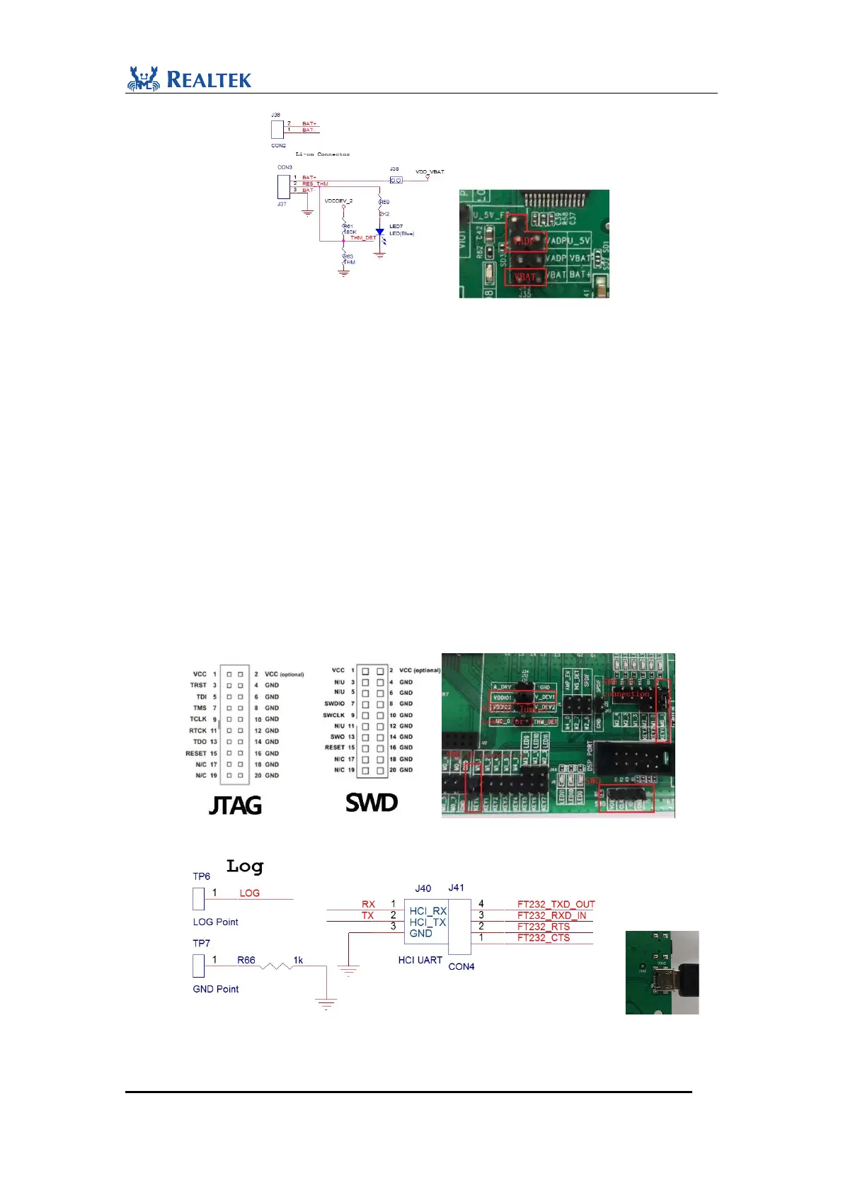
Figure2-1 Power Jumper Connection
2.2.2 Debug Interface
To download and debug APP program, follow the steps below:
1. J-Link is connected to corresponding SWD interface on motherboard as shown as follows.
Pay special attention to the consistency of working voltage between J-Link and
Motherboard. Keep VCC pin of J-Link floating if it is internal powered. It is suggested to
pull off internal jumper in J-link, and connect VDDIO1 which is powered through J32 to
VCC pin of J-link (Pin1).
In boot code, M2_0 is configured to transmit asynchronous data output as debugging
log information in UART protocol. Check bottom side of Evaluation board to confirm
whether built-in FT232 chip is mounted as shown as follows. If yes, follows the steps:
1. Connect TP6 and J41.3, and connect USB connector CON3 on bottom side to PC as USB
to UART input.
Figure 2-2 SWD interface connection
Figure 2-3 Connection for USB to UART converter