Renesas RA Family AIK-RA6M3, v1 User's Manual
R12UZ0143EE0100 Rev.0.1 Page
of 25
Oct.15.23
5.2.3 MCU Boot Mode
A two-pin header (J15) is provided to select the Boot Mode of the MCU. For normal operation, or Single-
Chip Mode, leave J15 open. To enter SCI Boot Mode or USB Boot Mode, place a jumper on J15.
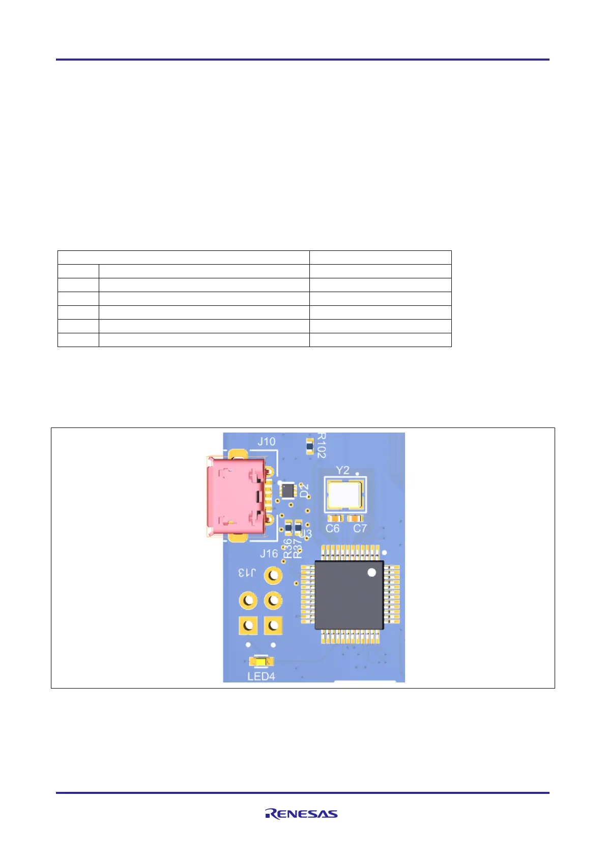
5.2.4 Debug Interface
The AIK-RA6M3 Debug Interface has two operating modes: (1) Onboard Debug using the Renesas RA4M2
microcontroller J-Link On-Board, 2) External Debug using the JTAG connector(J12).
The J-Link OB USB Micro-B connection jack (J10) connects the Renesas RA4M2 J-Link MCU to an external
USB Full Speed Host, allowing re-programming and debugging of the Main MCU firmware. This is the default
debug mode for AIK-RA6M3.
The Renesas RA4M2 J-Link MCU connects to the Main MCU using the SWD interface.
Table 2. Debug USB Connector (J10)
USB ID, jack internal switch, cable inserted
A yellow indicator LED4 provides a visual status of the state of the debug interface. When AIK-RA6M3 is
powered on, and LED4 is blinking, this indicates that the RA4M2 J-Link OB is not connected to a
programming host. When LED4 is on solid, this indicates that the RA4M2 J-Link OB is connected to a
programming interface.
Figure 7. AIK-RA6M3 Debug Interface
5.2.4.1 External Debug
One 10-pin Cortex
®
Debug Connector is provided at J12, which supports JTAG and SWD. This connector
may be used for external debug of the Main MCU.

 Loading...


