of 25
Oct.15.23
Table 12. AIK-RA6M3 Switches ...................................................................................................................... 18
Table 13. Ethernet Port Assignments .............................................................................................................. 20
Table 14. Ethernet Components ...................................................................................................................... 20
Table 15. MICs Port Assignments ................................................................................................................... 20
Table 16. CAN Port Assignments .................................................................................................................... 21
Table 17. Camera Module Socket ................................................................................................................... 21
Table 18. AIK-RA6M3 Design Package Contents ........................................................................................... 23
1. Kit Overview
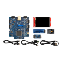
The AIK-RA6M3 enables developers to get started with initial firmware development. For more information
on the AIK-RA6M3, see www.renesas.com/AIK-RA6M3.
The kit includes breakout pin headers for direct access to the RA6M3 microcontroller I/O pins. On-board
support is included for several of the most commonly used peripherals, as well as interfaces for several
common ecosystem standards.
• Renesas RA6M3 Microcontroller Group
⎯ R7FA6M3AH3CFC
⎯ 176-pin LQFP package
⎯ 120 MHz Arm
®
Cortex
®
M4 core with FPU
⎯ 640 KB on-chip SRAM
⎯ 2 MB on-chip code flash memory
⎯ 64 KB on-chip data flash memory
• Connectivity
⎯ One USB micro AB full speed connector for the Main MCU
⎯ SEGGER J-Link
®
On-board (OB) interface for debugging and programming of the RA6M3 MCU. A 10
pin JTAG/SWD interface are also provided for connecting optional external debuggers and
programmers.
⎯ Six PMOD connectors, allowing use of appropriate PMOD compliant peripheral plug-in modules for
rapid prototyping
⎯ One Auxiliary Port connector
⎯ One CAN interface
⎯ One RJ-45 RMII Ethernet interface
• Multiple clock sources
⎯ Main MCU oscillator crystals, providing precision 24.000 MHz and 32,768 Hz reference clocks
⎯ Additional low-precision clocks are available internal to the Main MCU
• MCU reset push button switch
• Two user push button switches, monitored by Main MCU firmware
• One Dip switch
• Operating voltage
⎯ External 5 V input through any of the USB connections
• A Blue LED indicating availability of regulated power
• One LED RGB , controlled by the Main MCU firmware
• MCU boot configuration jumper

 Loading...