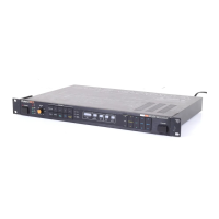
Do you have a question about the Roland SDE-1000 and is the answer not in the manual?
Provides an overview of the digital delay line technology and its comparison to tape echo machines.
Details the function and gain range of the head amplifier circuit.
Describes the audio signal routing and mixing stages within the unit.
Explains the circuit stage that boosts higher frequency components for improved S/N ratio.
Details the Sample and Hold circuit's role in extracting signal portions for A/D conversion.
Explains the Analog-to-Digital converter process and its components.
Describes the first low-pass filter stage, including its anti-aliasing function.
Details the stage that logarithmically reduces the signal's dynamic range.
Explains the Digital-to-Analog conversion process for reconstructing delayed audio.
Describes the circuit that amplifies delayed audio to restore its original dynamic range.
Describes the second low-pass filter stage, providing smoothing after digital conversion.
Explains how this stage compensates for preemphasis, restoring flat frequency response.
Details the circuit that reverses the delay output phase relative to the direct signal.
Describes the central gate array controlling all digital delay sequences.
Details the specific pin functions of the main controller IC.
Explains how data is handled and shifted for memory access.
Details the address pins used for accessing RAM memory cells.
Explains the Row Address Strobe signal for RAM access.
Details the Column Address Strobe signals for RAM access.
Provides a visual block diagram of the main controller's internal structure.
Illustrates the timing relationships of signals related to the main controller.
Explains the clock signals and generator responsible for timing operations.
Describes the Central Processing Unit and its role in retaining settings.
Details the specific head amp circuit and gain range for the SDE-3000.
Describes the delay output stage and its phase selection capability.
Explains the mixed output stage and its gain variation with UNIGAIN settings.
Details the Control Voltage input stage and its level shifting function.
Describes the inverted output stage and its level shifting function.
Explains how the modulation depth is controlled by external CV input.
Details the companding process used for audio signal digitization in the SDE-3000.
Describes the CV linearizer circuit for compensating nonlinear V/C characteristics.
Details the main controller IC specific to the SDE-3000 model.
Explains the function of peak hold and comparator circuits for signal analysis.
Identifies the RAM modules used for sound storage and their organization.
Details control signals and their states in various operational modes.
Initial troubleshooting steps to diagnose delay sound issues and check circuit functionality.
Procedure to disconnect the companding circuit for fault isolation.
Troubleshooting steps for issues related to the companding circuit's operation.
Method for identifying faulty RAM groups based on delay time settings.
Testing RAM states by applying constant input levels to check for stuck bits.
Procedure for isolating specific faulty RAM modules within the delay system.
Procedure for calibrating the input and output level meters.
Steps for adjusting the delay time settings and display accuracy.
Procedure for adjusting the compressor's level linearity.
Steps for adjusting the compressor to minimize total harmonic distortion.
Procedure for adjusting the expander to minimize total harmonic distortion.
Steps for adjusting the unit's frequency response across different settings.
Procedure for adjusting the feedback level and ensuring proper decay.
Adjusting the D/A converter output offset for accurate signal reproduction.
Procedure for verifying the correct DC supply voltages within the unit.
Steps for calibrating the input level meter to its specified accuracy.
Procedure for adjusting the Voltage Controlled Oscillator's frequency.
Adjusting the rate of the Low Frequency Oscillator for modulation effects.
Steps for adjusting the unit's frequency response across different settings.
Procedure for adjusting the feedback level and ensuring proper decay.
Adjusting the D/A converter output offset for accurate signal reproduction.
| Brand | Roland |
|---|---|
| Model | SDE-1000 |
| Category | Recording Equipment |
| Language | English |