CV10
Quick Start Guide
SEPTEMBER 2004 4
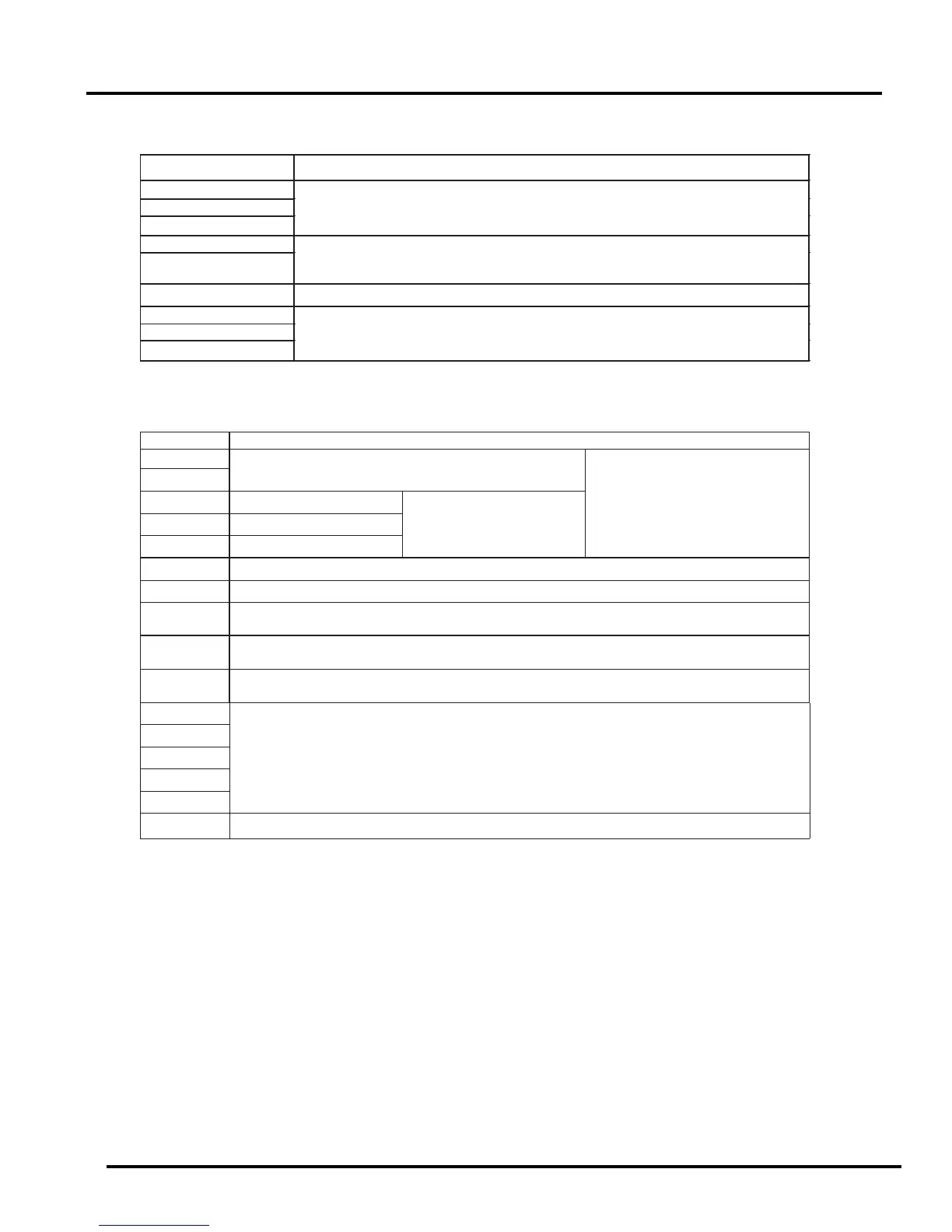
Descriptions of CV10 Main Circuit Terminals
Terminal Description
L1 ( L )
L2
L3 ( N )
Main power input: Single-phase: L/N
Three-phase: L1/L2/L3
P1
BR
Braking resistor or connecting terminal: Used in cases where the
drive frequently trips due to large load inertia or short
deceleration time (refer to specifications of braking resistor)
P1 and P DC reactor connecting terminals
T1
T2
T3
Drive output
Descriptions of CV10 Control Circuit Terminals
Terminal Description
R2A
R2B
Multifunctional output terminal - Normally open
R1C Common contact
R1B Normally close contact
R1A Normally open contact
Multifunctional terminals –
Normally open
Contact rated capacity:
(250VAC/1A or 30VDC/1A)
Contact using description: (refer to
8-02, 8-03)
10V Speed Potentiometer (VR) power source terminal (referenced to COM)
AIN Analog frequency signal input terminal (refer to 5-06 description)
24V
Common contact for S1~S5 in PNP (source) input. (refer to CV10 wiring diagram) of SW1
when PNP input is used.
COM
Common contact for S1~S5 in NPN (sink) input. (refer to CV10 wiring diagram) of SW1 when
NPN input is used.
FM+
The positive analog output for multifunction (refer to 8-00 description),
the signal for output terminal is 0-10VDC
S1
S2
S3
S4
S5
Multifunction input terminals(refer to 5-00 ~ 5-04 description)
S6/AV2 PID input terminal (refer to 5-05 description)