EasyManua.ls Logo

Samsung DSR9500 VIA CI User Manual

Samsung DSR9500 VIA CI
41 pages
To Next Page IconTo Next Page
Page #1 background imageLoading...
Page #1 background image
DIGITAL SATELLITE RECEIVER
DSR9500 FTA
DSR9500 CI
DSR9500 EM VIA
DSR9500 VIA CI
SERVICE
1. Precautions
2. Operating Instructions
3. Software Upgrade and Installation
4. Troubleshooting
5. Exploded View and Parts List
6. Electrical Parts List
7. PCB Diagrams
8. Schematic Diagrams
Manual
DIGITAL SATELLITE RECEIVER CONTENTS
SERVICE MANUAL DSR9500 (FTA, CI, EM VIA, VIA CI)
ELECTRONICS
© Samsung Electronics Co., Ltd. APR. 2002
Printed in Korea
MF82-00001A
Question and Answer IconNeed help?

Do you have a question about the Samsung DSR9500 VIA CI and is the answer not in the manual?
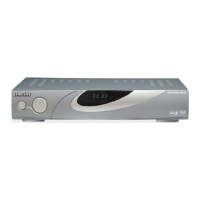
Samsung DSR9500 VIA CI Specifications

General IconGeneral
Conditional AccessVIA CI
Input Frequency Range950 - 2150 MHz
CI Slot1
TypeSatellite Receiver
Input Impedance75 Ohms
LNB Power13/18V, 500mA
DiSEqC1.0
Video DecoderMPEG-2
Audio DecoderMPEG-1, MPEG-2
Audio OutputRCA

Summary

Precautions

Operating Instructions

Software Upgrade and Installation

Troubleshooting

Troubleshooting: No Power (LED Off)

Diagnostic steps for when the device has no power and the LED is off.

Troubleshooting: No Locking

Diagnostic steps for when the receiver does not lock onto a signal.

Troubleshooting: No RF-Mod Output

Steps to diagnose issues with the RF modulator output.

Troubleshooting: No SPDIF Output

Steps to diagnose issues with the SPDIF digital audio output.

Troubleshooting: No S-Video Output

Steps to diagnose problems with the S-Video output signal.

Troubleshooting: No Video (TV SCART, RCA)

Diagnostic steps for missing video signals on SCART or RCA outputs.

Troubleshooting: No Video Out (VCR)

Steps to diagnose issues with the VCR video output.

Troubleshooting: No Audio Out

Diagnostic steps for when there is no audio output from the receiver.

Exploded View and Parts List

Electrical Parts List

PCB Diagrams

7-1 Main PCB Diagram

Detailed diagram of the main Printed Circuit Board.

7-2 Front PCB Diagram

Diagram for the front Printed Circuit Board assembly.

Schematic Diagrams

Related product manuals