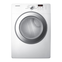
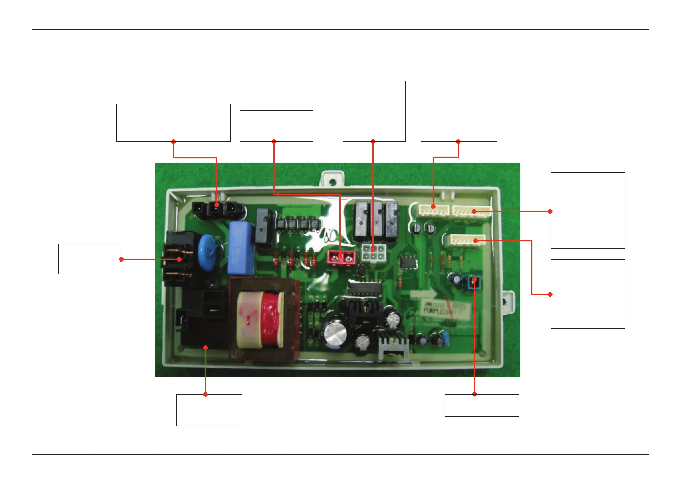
74 _ PCB Diagram
6-2. DETAILED DESCRIPTIONS OF CONTACT TERMINALS (MAIN PCB)
► RY6
1.HeaterRelaySwitch
2.HeaterRelaySwitch
► CN1
1.ACPowerPort
2.ACPowerOffDetectionSensor
3. Door Detection Sensor (LOCK, UNLOCK)
► RY5
1.MotorRelaySwitch
2.MotorRelaySwitch
► CN7
1. Reactor Connection Port
2. Reactor Connection Port
► CN5
1.SteamValve1
2. Empty Pin
3. LAMP
4. Empty Pin
5.SteamValve2
6. Empty Pin
► CN2
1.CommunicationsPort(Tx)
2.CommunicationsPort(Rx)
3.SubReset
4. DGND
5.5V
6.15V
► CN3
1.5V
2. SO
3. SI
4. RESET
5. CLOCK
6. FLMDO
7. DGND
8. Empty Pin
► CN4
1. DGND
2. Empty Pin
3. Temperature Sensor
4.FabricDetectionSensor
5.FabricDetectionSensor
6.5V
7.5V
► CN6
1. SET GND