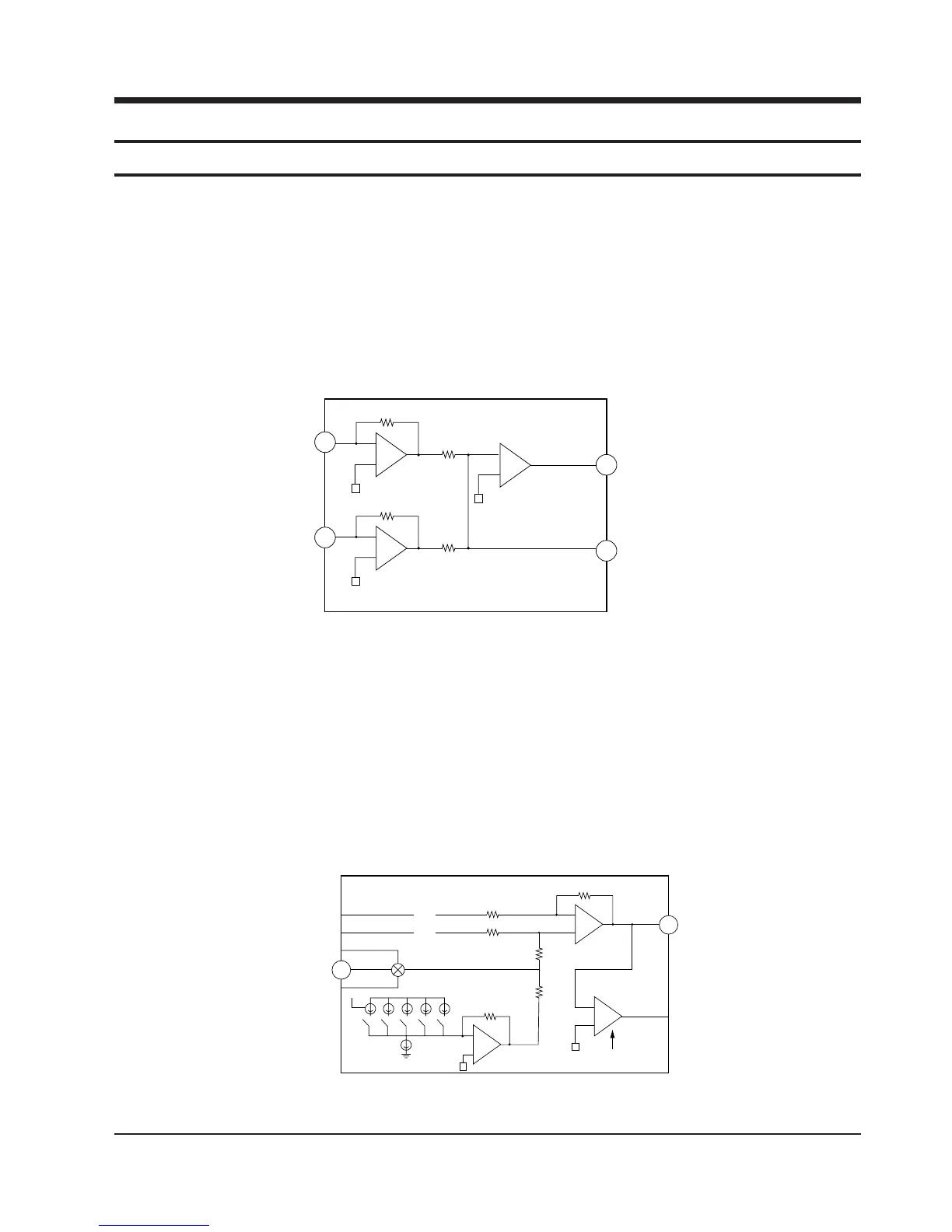
The two currents from input pins PD1 (A+C) and PD2 (B+D) are converted into voltages through I/V Amp,
and they are added to RF summing Amp. The photo diode (A+B+C+D) signal which is I-V changed is
outputted by RFO (pin74). At this pin, the eye pattern can be checked.
The output of the focus error amp is the difference between RF I-V AMP(1) output Va and RF I-V AMP(2)
output Vb,just is the Photo Diode ((A+C) - (B+D)) signal which is I-V changed.
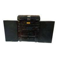
The focus error bias voltage applied to the (+) of focus error amp can be changed by D/A converter as shown
in diagram, so that the offset of focus error amp can be adjust automatical.
Focus error bias can be adjusted from the range of +100mV ~ -100mV by connectiong the resistor with pin 63
(FEBIAS).