– 2 –
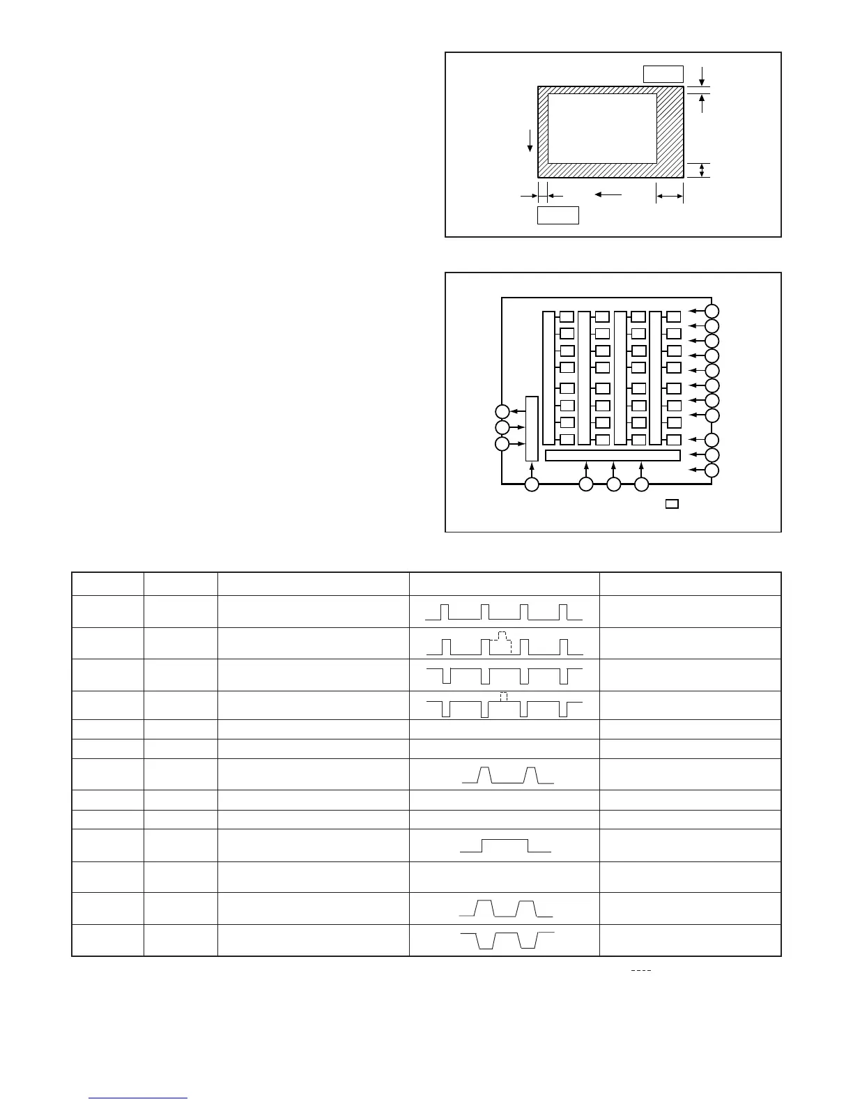
Fig. 1-1.Optical Black Location (Top View)
Pin No.
Symbol Pin Description
Waveform
Voltag e
Table 1-1. CCD Pin Description
When sensor read-out
Fig. 1-2. CCD Block Diagram
1. OUTLINE OF CIRCUIT DESCRIPTION
1-1. CP1 CIRCUIT DESCRIPTION
1. IC Configuration
IC903 (MN39620PJJ) CCD imager
IC901 (AN20101A) V driver
IC906 (AD9948KCPZ) CDS, AGC, A/D converter
2. IC903 (CCD)
[Structure]
Interline type CCD image sensor
Optical size 1/2.5 type format
Effective pixels 2620 (H) X 1984 (V)
Pixels in total 2690 (H) X 1994 (V)
Optical black
Horizontal (H) direction: Front 12 pixels, Rear 58 pixels
Vertical (V) direction: Front 8 pixels, Rear 2 pixels
Dummy bit number Horizontal : 28 Vertical :1
1
4, 7
5, 6
9
V
3B, V3A
V4, V2
Vertical register transfer clock
Vertical register transfer clock
Signal output
-6.0 V, 0 V, 12 V
Aprox. 9 V
Vertical register transfer clock
VOUT
V
6
-6.0 V, 0 V
-6.0 V, 0 V
GND
Reset gate clock
GND
Circuit power
DC
12 V
GND 0 V
H-L 3.4 V
ØR
10
11
12
VDD
DC
Protection transister bias
-6.0 V
PT
DC
H
L, H1
Horizontal register transfer clock
Substrate clock
DC
SUB
0 V, 3.5 V
13
15
16, 17
H
2
Horizontal register transfer clock
0 V, 3.5 V
18
2, 3, 8
V
5B, V5A, V1 Vertical register transfer clock
Substrate controlSUBSW
14
0, 3.3 V (When importing all
picture element: 3.3 V)
-6.0 V, 0 V, 12 V
Aprox. 6 V
(Different from every CCD)
Pin 10
2
8
58
12
H
V
Pin 1
17
18
11
16
øR
øHL
øH1
øH2
: Photo diode
Output part
9
VOUT
10
VDD
12
GND
8
7
øV2
1
2
3
4
5
6
øV3A
Vertical shift register
Horizontal shift register
øV3B
øV4
øV5A
øV5B
øV6
15
SUB
14
SUBSW
13
PT
øV1
 Loading...