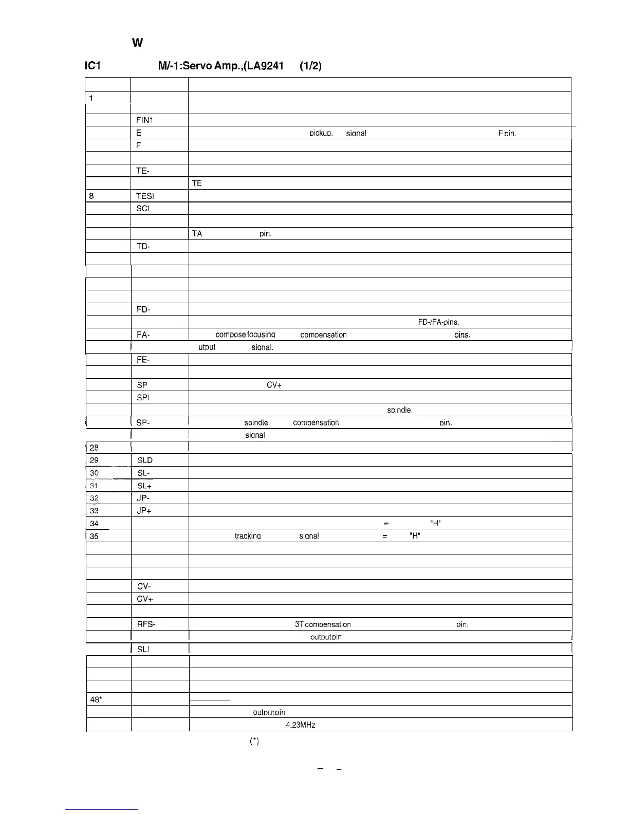
CD-C471 W
ICl
VHiLA9241 M/-l
:Servo
Amp.,(LA9241
M)
(i/2)
Pin No.
Port Name
Function
1
FIN2
Connection pin for photodiode of pickup.
RF signal is generated through addition with FIN pin, and FE signal is generated through subtraction.
2
FIN1
Connection pin for photodiode of pickup.
3
E
Connection pin for ohotodiode of
pickuo.
TE
sianal
is aenerated throuah subtraction with
F
Din.
4
F
5
TB
6
TE-
7
TE
8
TESI
9
SCI
10
TH
11’
TA
Connection pin for photodiode of pickup.
Pin for input of DC component of TE signal.
Pin to connect gain setting resistor of TE signal to TE signal.
TE
signal output pin.
TES (Track error sense) comparator input pin. TE signal is band-passed and input.
Input pin for shock detection.
Pin to set time constant of tracking gain.
TA
amplifier output
Din.
12
TD-
13
TD
Pin to compose tracking phase compensation constant between TD and VR pins.
Pin to set tracking phase compensation.
14
JP
15
TO
16
FD
17
FD-
18
FA
19
FA-
Pin to set amplitude of tracking jump signal (kick pulse).
Tracking control signal output pin.
Focusing control signal output pin.
Pin to compose focusing phase compensation constant between FD and FA pins.
Pin to compose focusing phase compensation constant between
FD-/FA-pins.
Pin to
comoose
focusina
phase
comoensation
constant between FA and FE
Dins.
20
1
FE
lo
LItPUt
pin of FE
sional.
21
FE-
22
AGND
23
SP
24
SPI
25
SPG
1
26
I
SP-
Pin to connect gain setting resistor of FE signal across TE pin.
GND for analog signal.
Single end output for
CV+
and CV- pin input.
Spindle amplifier input.
Pin to connect aain settina resistor in the 12cm mode of
soindje.
I
Pin to connect
soindte
phase
comoensation
constant toaether with SPD
oin.
I
27
1
SPD
I
Spindle control
sianal
output pin.
I
28
/
SLEQ
I
Pin to connect thread phase compensation constant.
Thread control signal output pin.
Input pin of thread feed signal from micro computer.
input pin of thread feed signal from micro computer.
JP-
JP+
TGL
TOFF
36
TES
37
HFL
38
SLOF
39
cv-
40
cv+
41
RFSM
42
RFS-
Input pin of tracking jump signal from DSP.
Input pin of tracking jump signal from DSP.
input pin of tracking gain control signal from DSP. TGL
=
Gain low at
“H”
Input pin of
trackina
off control
sianal
from DSP. TOFF
=
Off at
“H”
Output pin of TES signal to DSP.
(HIGH FREQUENCY LEVEL) is used to judge whether main beam is positioned on the bit or on the mirror.
Thread servo off control input pin.
Pin to input CLV error signal from DSP.
Pin to input CLV error signal from DSP.
RF output pin.
Pin to set aain of RF and set
3T
comoensation
constant toaether with RFSM
Din.
43
I
SLC
I
(SLICE LEVEL CONTROL) is the
outout
Din
to control of the level of the data slice with RF waveform DSP.
I
I
44
I
SLI
I
Input pin to control the level of data slice with DSP.
45
DGND
46
FSC
47
TBC
MS*
NC
49
DEF
GND pin in the digital system.
Output pin for focus search smoothening capacitor.
(Tracking Balance Control) Pin to set EF balance variable range.
Defect detection
outout
Din
of disk.
50
CLK
Reference clock input pin.
4.23MHz
of DSP is input.
In this unit, the terminal with asterisk mark
(*)
is (open) terminal which is not connected to the outside.
-
46
-