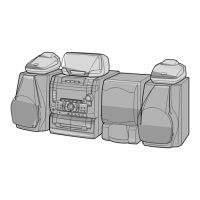
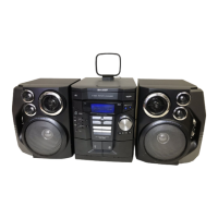
CD-K1861V
– 58 –
Pin No.
Terminal Name
Function
1 Clamp input terminal Input of 1.9 V clamp, 1 Vp-p composite or Y-signal
2 GND Ground
3 Sag correction terminal Able to obtain an output without any sag by feeding back the sag, generated from output
coupling C, using the external C (see block diagram).
When not using the sag correction terminal, connect directly to the pin 4.
4,5 Output terminal 6 dB amplifier output. Able to drive 75? line.
6 Sag correction terminal Able to obtain an output without any sag by feeding back the sag, generated from output
coupling C, using the external C (see block diagram).
When not using the sag correction terminal, connect directly to the pin 5.
7 V+ Power source
8 Clamp input terminal Input of 1.9 V clamp, 1 Vp-p composite or Y-signal.
ICV4 VHiNJM2267M-1: Video Operation Amp. (NJM2267M)
6dB
Amp
6dB
Amp
75Ω
Driver
75Ω
Driver
Vout2
75Ω
2.2Ω
2.0kΩ
Vout1
75Ω
V5AG2
V5AG1
GND
2.2kΩ
2.0kΩ
Clamp
Clamp
7
5
6
4
3
2
1
8
VIN2
VOUT2
(6dB)
VOUT2
VOUT1
(6dB)
VOUT1
V+
VIN1
Correction terminal
Correction terminal
Figure 58 BLOCK DIAGRAM OF IC
ICV2 VHiD61012GC-1: MPEG Decoder (D61012GC) (3/3)
CBP3-
CBP1
VOUT3-
VOUT1
VCLK
HSYNC
NSYNC
CSYNC
AUDO
AUBCK
AULRCK
AUEMPH
AUCLK
MWE
MCAS
MRAS
MA8-0
MD15-0
X1 X2
RESET
INT
HSELA
HSELX
HDAK
HWR
HRD
HCS
HA
HD7-HD0
CDC2P0
CDEMPH
CDLRCK
CDBCK
CDI
CD-DSP
INTERFACE
SRAM
CD-ROM
DECODER
SRAM
OSD
NTSC/PAL
encoder
3ch
VIDEO
DAC
DRAM interface
A/V
sepa-
ration
Host interface
System
control
Video
decoder
Inter-
lace
Video interface
Synchronized signal
generating circuit
Audio
decoder
Audio
interface
Arbiter
2-5,7-10
22
19
20
21
28
23
24
54-56,
58-62,
65-68,
70-73
49
53
52
38-42,
45-48
29 27
13
14
80
35
32
33
34
31
79
78
77
86,88,90
85,87,89
95-99