-
-
----
-3
.9
V
VDISP
VB
---
-
--
-2
.
lV
- - -
--
-
-
3.
9V
L_
VM
-
-
-----IV
...._
__ - - -
--
- -
2.8
V
6.8ms--
--
VA
-- ---
ov
...._
__ - - -
--
-
-
I.
8
V
11
E
ye
po
siti
on
30
°
o
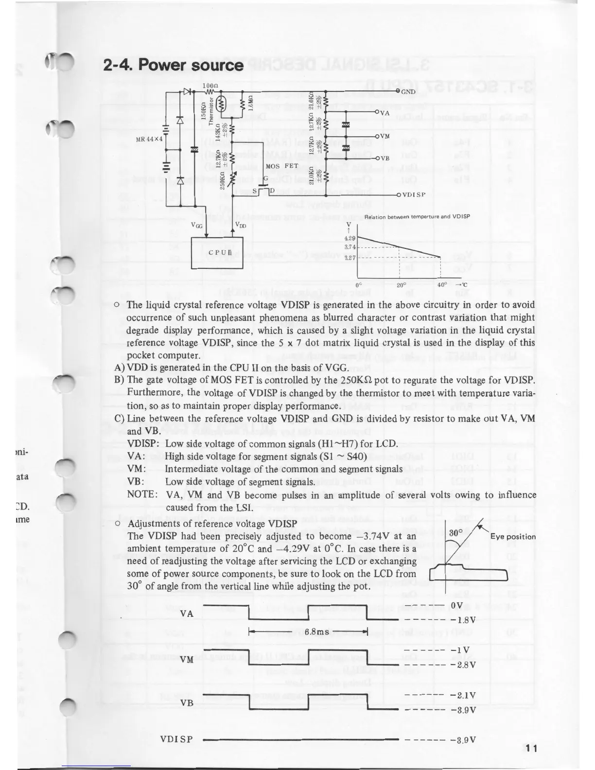
Adj
u
stments of reference voltage VD ISP
The VDISP had been precisely adjusted to become
-
3
.
74V at an
ambi
e
nt temperature of
20
°
C
and
-
4
.
29V at
0
°
C
.
In case there
is
a
n
eed of
rea
d
justing the voltage after servicing the LCD or exchanging
some of power source
components
,
be sure to look on the LCD from
30° of angle from the
v
e
rtical line while adjusting the pot.
:
D
.
mi-
Low side voltage of common signals
(Hl-H7)
for
LCD
.
High side voltage for segment signals
(S
l
-
S40)
Intermediate voltage of the common and
segm
e
nt signals
Low side voltage of segment signals.
VA
,
VM and VB become pulses in an amplitude of several volts owing to influence
caused from the LSI.
VA:
VM:
VB
:
NOTE
:
ata
o The
liq
ui
d
cry
s
tal
refer
e
nce voltage
VDI
S
P
is
generated in the above
circ
ui
try in order to
avoi
d
occurrence of such unpleasant phenomena
as
blurred character or contrast
var
i
ation that might
degrade display
performance
,
which
is
caused by
a
slight voltage variation in the liquid crystal
refer
e
nce voltage VD ISP, since the
5
x
7
dot matrix liquid crystal
is
use
d
in the
di
sp
lay of this
pock
e
t
com
pu
ter.
A)
VD
D
i
s
generated in the CPU
II
on the basis of VGG.
B) The gate
vo
l
tag
e
of MOS FET
i
s
controlled by the 250KS1 pot to regurate the voltage for VDISP.
Furthermore
,
the voltage of VDISP
is
changed by the thermistor to meet with temperature
varia
-
tio
n
,
so as to maintain proper display
performance
.
C) Line between the reference voltage VD ISP and GND
is
d
ivided by resistor to make
o
u
t VA, VM
an
d
VB
.
V
DISP
:
2
0
°
o
o
C
PU
il
Yoo
Relation between
ternperture
and
VD
I
S
P
M
OS FET
ioo»
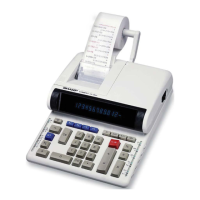
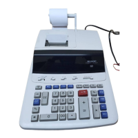
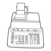
2-4. Power source