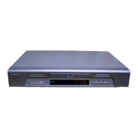
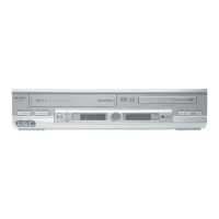
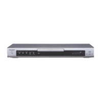
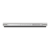
DV-600S
DV-600H
Pin No. Terminal name I/O Operation function
1 EIN I RF signal input. Input of RF signal output of optical pickup.
2 GND1 – Ground
3 S/DUAL I Single layer/dual layer selection signal input.
4 AIN I RF signal input. Input of RF signal output of optical pickup.
5 BIN I RF signal input. Input of RF signal output of optical pickup.
6 CIN I RF signal input. Input of RF signal output of optical pickup.
7 DIN I RF signal input. Input of RF signal output of optical pickup.
8 VrefIN I Reference voltage input. (2.1V)
9 FIN I RF signal input. Input of RF signal output of optical pickup.
10 GAINsel1 I Amp gain selection input 1.
11 VCC1 – Power terminal. (5.0V)
12 GAINsel2 I Amp gain selection input 2.
13 FOUT O RF signal output. Input RF signal is current-voltage-converted and output.
14 EOUT O RF signal output. Input RF signal is current-voltage-converted and output.
15 DOUT O RF signal output. Input RF signal is current-voltage-converted and output.
16 COUT O RF signal output. Input RF signal is current-voltage-converted and output.
17 BOUT O RF signal output. Input RF signal is current-voltage-converted and output.
18 AOUT O RF signal output. Input RF signal is current-voltage-converted and output.
19 VCC2 – Power terminal. (5.0V)
20 RFPOUT O Data read signal output. The same phase as MIXIN.
21 RFNOUT O Data read signal output. Reverse phase with respect to MIXIN.
22 MIXIN I Data read signal input.
23 MIXOUT O Data read signal output.
24 GND2 – Ground
• Block Diagram
• Mode selection table
GAINsel1 (Terminal 10) GAINsel2 (Terminal 12) Amp gain
L L +6dB
H, OPEN L -2dB
L H, OPEN +2dB
H, OPEN H, OPEN -6dB
Amp. gain selection
Layer S/DSEL (Terminal 3) Amp gain
Single L, OPEN 0dB
Dual H +10dB
Single layer/dual layer selection
11-2. IC301 IX1461GE RF PRE AMP.
H, V
Y
demux
Cb
Cr
Modulator
subcarrier
gen
off_set
0
0
0
CGMS,
WSS gen
CC_gen
Sync_generator
BG
copy
protection
bus
bus
TESTI2C/SPI
BIAS
DAC
DAC
DAC
30 37, 57
28
51
38, 56
39~46
52~55, 58~61
DVdd
DVss
DVIA [7:0]
DVIB [7:0]
A/B_sel
62
TP
29
Clock
26
Chip A
31
Reset
32
33
PAL/NTSC
SO
34
SDA/SI
35
SCL/SCK
36
SEL
27
TEST
10
DAVss
13
DAVdd
15
Ibias 2
14
Vref 2
24
C/Cr/R 2
23
C/Cr/R 2
18
CVBS/Cb/B 2
17
CVBS/Cb/B 2
21
Y/G 2
20
Y/G 2
11
Ibias 1
12
Vref 1
8
C/Cr/R 1
7
C/Cr/R 1
2
CVBS/Cb/B 1
1
CVBS/Cb/B 1
5
Y/G 1
4
Y/G 1
9
C/Cr/R 1Vdd
3
CVBS/Cb/B 1Vdd
6
Y/G 1Vdd
25
C/Cr/R 2Vdd
19
CVBS/Cb/B 2Vdd
22
Y/G Vdd
50
Hsync
49
F/Vsync
48
C/Fsync/VBI
MC44724/5A
BIAS
DAC
DAC
Output Selector
DAC
0
0
0
0
0
0
0
RGB matrix
11-2