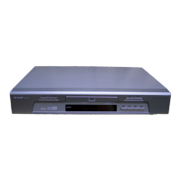
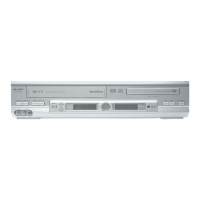
DV-600S
DV-600H
11-5. IC402 IX1474GE DEM/ECC (DVD)
Pin No. Terminal name I/O Operation function Remarks
1 DPCK1 I Signal processing reference clock input. 0.5-3.3Vp-p Feedback
resistor built in.
2 DVDD3 – Digital power. (3.3V) For logic cell
3 SVCK1 I Servo reference clock input. (Oscillation circuit input terminal) 3.3V-I/F Feedback
4 SVCK0 O Servo reference clock output. (Oscillation circuit input terminal) resistor built in.
5 DVSS – Digital power. (0V) For logic cell
6 DVDD2 – Digital power. (3.3V) For logic cell
7 N.C. – User use prohibited. Open
8 HDWR I MPU write signal. TTL level
9 HDRD I MPU read signal. TTL level
10 ECCCS I MPU chip selection. TTL level
11 D8 I/O MPU data bus. TTL level
12 D9 I/O MPU data bus. TTL level
13 D10 I/O MPU data bus. TTL level
14 D11 I/O MPU data bus. TTL level
15 D12 I/O MPU data bus. TTL level
16 D13 I/O MPU data bus. TTL level
17 D14 I/O MPU data bus. TTL level
18 D15 I/O MPU data bus. TTL level
19 DVSS – Digital power. (0V) For I/O cell
20 DVDD5 – Digital power. (5V) For I/O cell
21 HINT O MPU interruption signal. (Occurrence of interruption = “L”) OPEN DRAIN
22 HA0 I MPU address bus. TTL level
23 HA1 I MPU address bus. TTL level
24 PLCK I/O Read channel clock input/output terminal.
25 ED0 – User use is prohibited (N.C.) since it is for shipping adjustment. Open
26 ED1 –
27 ED2 –
28 ED3 –
29 ED4 –
30 ED5 –
31 ED6 –
32 ED7 –
33 TEST I For shipping adjustment. Set to “L”
34 PDON O PLL phase error signal output. (Negative polarity)
35 PDOP O PLL phase error signal output. (Positive polarity)
36 RLLD O RLL detection result output.
37 LPFN I PLL loop filter amp. reverse input.
38 LPFO O PLL loop filter amp. output.
39 VCOF O VCO filter terminal.
40 SLCO O Built-in comparator reference voltage output terminal.
41 AVSS – Analog power. (0V)
42 AVR O Non-PLL system analog reference potential. (1.65V)
43 VRC – Resistance division point potential. (For analog reference
potential generation: 1.65)
44 PVR O PLL system analog reference potential. (1.65V)
45 AVDD – Analog power. (3.3V)
46 RVR2 – 2nd reference voltage. (For capacitor connection)
47 RVDD – Exclusive-use power terminal. (3.3V)
48 RFIN I RF signal input.
49 RVSS – Exclusive-use power terminal. (0V)
50 RVR1 – 1nd reference voltage. (For capacitor connection)
51 DVR I DMO reference potential. (1.65V recommended)
52 DMO O Disc equalizer output for DVD. (Triple value PWM + HiZ)
53 RASN O External RAM row address selection. (Negative logic)
54 CASN O External RAM row address selection. (Negative logic)
11-5


 To Next Page