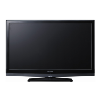
LC-26SB25E/S/RU, LC-32SB25E/S/RU, LC-42SB55E/S/RU
66
20 TSSYNC O TS packet start signal
21 TSCLK O TS output clock
Analog Signal
6 RSSI_IN A Received signal strength indicator input
43 IIN A Analog IF input (differential)
44 IIP A Analog IF input (differential)
47 REFTOP A ADC reference top voltage. Decouple with a capacitor to Analog ground plane.
45 REFBOT A ADC reference bottom voltage. Decouple with a capacitor to Analog ground plane.
46 VCMEXT A ADC common mode voltage
Clock Generation
3 XTALI A
4 XTALO A
Crystal input
Control Signals
33 GIO0 I/O GIO 0
36 RF_AGC I/O
1. GIO4
2. RF AGC control
31 XTALCLK_SEL1 I
30 XTALCLK_SEL0 I
clock (crystal) frequency selection
25 SCL I Host processor serial clock input
26 SDA I/O Host processor serial data pin
38 SCLT I Tuner serial clock output, 5 volt compatible
37 SDAT I/O Tuner serial data pin, 5 volt compatible
35 IF_AGC O IF AGC output
32 RESET_B I
Power reset pin, low active
Required reset timing is 15ms(after power stable), VIH=2.5V,VL=0.5V
Power Supply
12, 22, 28, 34 VDD33 P Digital power supply, tie to 3.3V
7, 24, 27, 40 VDD12 P Digital power supply, tie to 1.2V
8, 23, 29, 39 DGND P Digital ground, tie to digital ground plane
5, 42, 48 AVDD33 P Analog power supply, tie to 3.3V
1, 2, 41 AGND P Analog ground, tie to analog ground plane
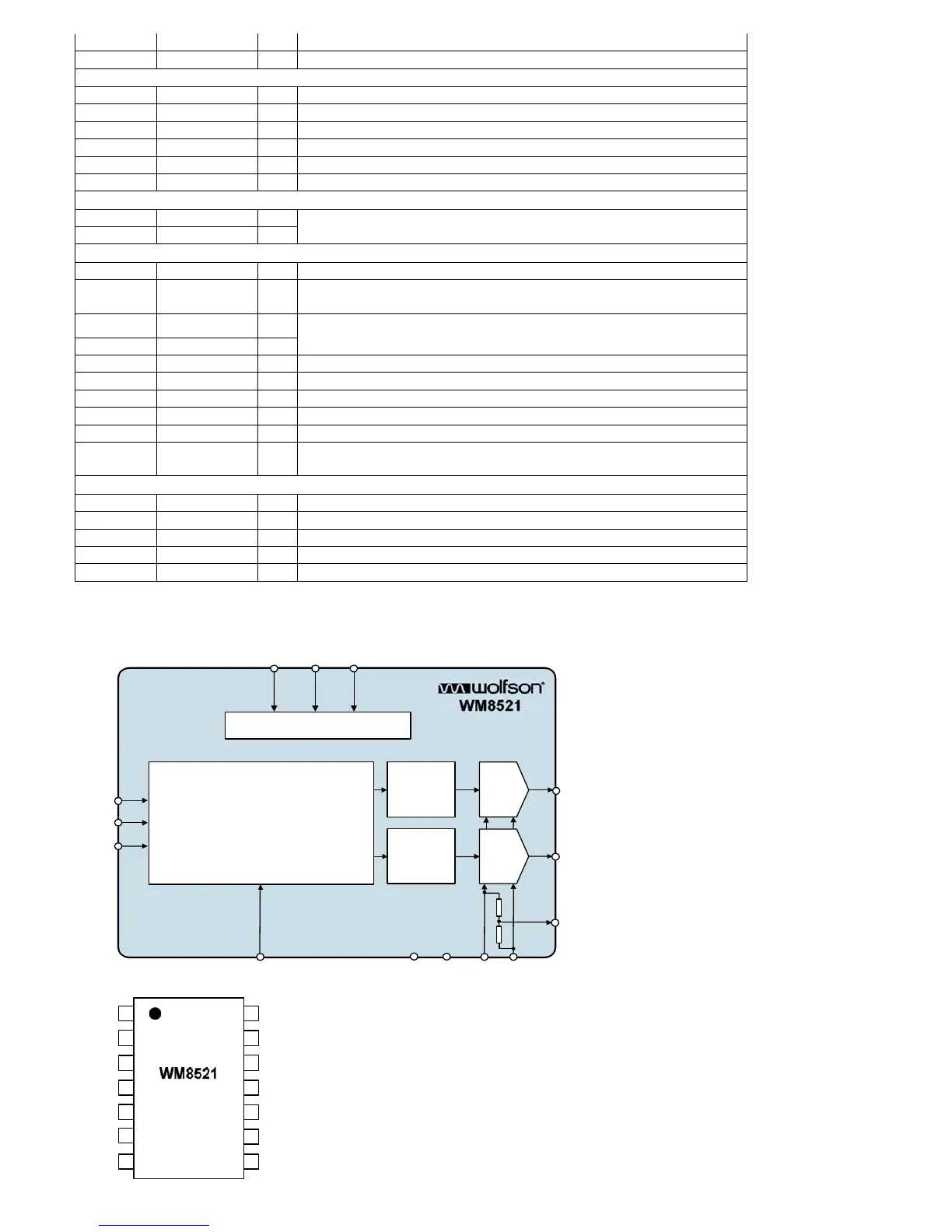
2.9. U602 (WM8521H9GED/RV SOIC-14)
2.9.1 Block Diagram
2.9.2 Pin Connections and short description
BCLK
LRCLK
DIN
FORMAT MUTE DEEMPH
CONTROL
INTERFACE
DIGITAL AUDIO
INTERFACE
&
DI G ITA L F ILT E RS
SIGMA
DELTA
MODULATOR
RIGHT
DAC
SIGMA
DELTA
MODULATOR
LEFT
DAC
VOUTR
VOUTL
CAP
DVDD DGND AVDD AGND
1
2
3
4
5
6
7
14
13
12
11
10
9
8
DGND
LRCLK
DIN
BCLK
MUTE
VOUTR
AGND
DVDD
MCLK
FORMAT
DEEMPH
VOUTL
AVDD
CAP
 Loading...