37
LC-40LE540
LC-46LE540
• Selectable clock input ratio.
• 96-kHz internal processing sample rate.
• Thermal overload and short-circuit protection technology
• Video apps: 576 x fs input mode supported.
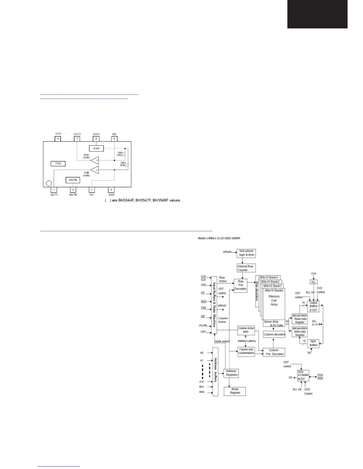
• IC 2702: Headphone Amplifier.
Part number: BH3547-E2
Sharp code : VHIBH3547F+-1L.
http://www.rohm.com/products/databook/audio/pdf/bh3541f-e.pdf
http://www.datasheetarchive.com/BH3541F-datasheet.html
BH3547F is a headphone amplifier suitable for portable products and includes a fixed gain of 6dB. Also it has mute functions that
make it easy to prevent pop noise when power supply turns on/off. Moreover, thermal shutdown function is built-in. Additionally,
the BH3547F can drive 16/32Ω loads.
• IC 3601 : DDRII FRC
Part number: H5PS5162GFR-S5C
Sharp code: RH-IXD361WJQZQ
http://www.hynix.com/products/graphics/view.jsp?info.ramKind=18&info.serialNo=H5PS5162FFR&posMap=EOL
• VDD/VDDQ= 2.0V +/- 0.1V(600/500 MHz)
• VDD/VDDQ= 1.8V +/- 0.1V(500/400 MHz)
• All inputs and outputs are compatible with SSTL_18 interface
• Fully differential clock inputs (CK, /CK) operation
• Double data rate interface
• Source synchronous-data transaction aligned to bidirectional data
strobe (DQS, DQS)
• Differential Data Strobe (DQS, DQS)
• Data outputs on DQS, DQS edges when read (edged DQ)
• Data inputs on DQS centers when write(centered DQ)
• On chip DLL align DQ, DQS and DQS transition with CK
transition
• DM mask write data-in at the both rising and falling edges of the
data strobe
• All addresses and control inputs except data, data strobes and data
masks latched on the rising edges of the
clock
• Programmable CAS latency from 3 to 7 supported
• Programmable additive latency 0, 1, 2, 3, 4, 5 and 6 supported
• Programmable burst length 4/8 with both nibble sequential and
interleave mode
• Internal four bank operations with single pulsed RAS
• Auto refresh and self refresh supported
• tRAS lockout supported
• 8K refresh cycles /64ms
• JEDEC standard 84ball FBGA(x16)
• Full strength driver option controlled by EMRS
• On Die Termination supported
• Off Chip Driver Impedance Adjustment supported
• Self-Refresh High Temperature Entry
• High Temperature Self Refresh rate supported
• Average Refresh Period 7.8us at lower than Tcase 85°C, 3.9us at 85°C<Tcase<95°C