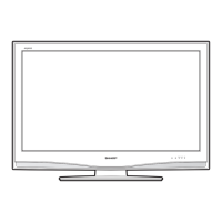
LC-42XL2E/S/RU, LC-46XL2E/S/RU, LC-46X20E/S/RU, LC-52XL2E/S/RU, LC-52X20E/S/RU
5 – 42
2.22. IC9602 (VHiMP2367DN-1Y)
2.22.1 Block Diagram
2.22.2 Pin Connections and short description
Pin No. Pin Name I/O Pin Function
1 BS I High-Side Gate Drive Boost Input. BS supplies the drive for the high-side N-Channel MOSFET switch.
Connect a 0.01µF or greater capacitor from SW to BS to power the high side switch.
2 IN I Power Input. IN supplies the power to the IC, as well as the step-down converter switches.
3 SW Drive IN with a 4.45V to 28V power source. Bypass IN to GND with a suitably large capacitor to eliminate noise
on the input to the IC.
4 GND Ground.
5 FB Feedback Input. FB senses the output voltage to regulate that voltage. Drive FB with a resistive voltage divider
from the output voltage. The feedback reference voltage is 0.8V.
6 COMP Compensation Node. COMP is used to compensate the regulation control loop. Connect a series RC network
from COMP to GND to compensate the regulation control loop. In same cases, an additional capacitor from
COMP to GND is required.
7 EN Enable Input. EN is a digital input that turns the regulator on or off. Drive EN high to turn on the regulator, drive
it low to turn it off.
8 SS Soft-start Control Input. SS controls the soft-start period. Connect a capacitor from SS to GND to set the soft-
start period.