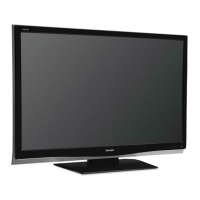
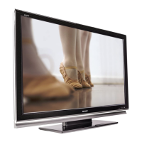
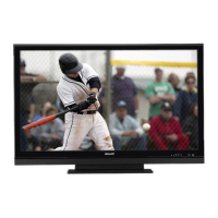
LC-42XL2E/S/RU, LC-46XL2E/S/RU, LC-46X20E/S/RU, LC-52XL2E/S/RU, LC-52X20E/S/RU
5 – 25
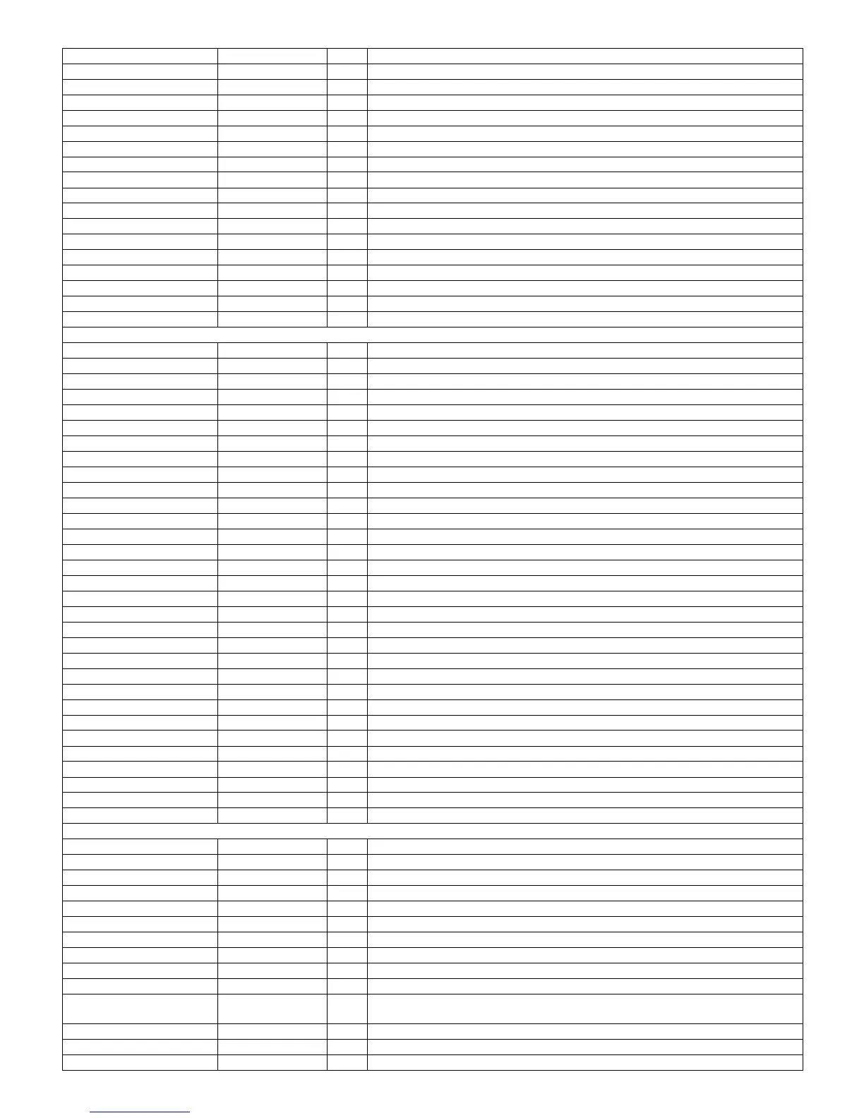
AP7 TD1P O LVDS Positive Output. (Not used)
AN7 TD1M O LVDS Negative Output. (Not used)
AP8 TCLK1P O LVDS Positive clock Output. (Not used)
AN8 TCLK1M O LVDS Negative clock Output. (Not used)
AP9 TC1P O LVDS Positive Output. (Not used)
AN9 TC1M O LVDS Negative Output. (Not used)
AJ4 LVDS_VDDO — LVDS Output buffer VDD (+3.3V).
AP10 TB1P O LVDS Positive Output. (Not used)
AN10 TB1M O LVDS Negative Output. (Not used)
AP11 TA1P O LVDS Positive Output. (Not used)
AN11 TA1M O LVDS Negative Output. (Not used)
AL5 LVDS_VSSO — LVDS Output buffer VSS.
AM5 LVDS_VDDO — LVDS Output buffer VDD (+3.3V).
AL3 LVDS_VSSA — LVDS Analog VSS.
AL4 LVDS_VDDA — LVDS Analog VDD (+3.3V).
AK3 LVDS_VSSD — LVDS Digital VSS.
AM3 LVDS_VDDD — LVDS Digital VDD (+3.3V).
PLL Interface
B7 DVSS22 — PLL ground related to DVDD22; supply for VCO circuit.
A7 DVDD22 — PLL power= 1.2V; supply for VCO circuit.
A6 DVSS21 — PLL ground related to DVDD21; supply for digital circuit.
B6 DVDD21 — PLL power= 1.2V; supply for digital circuit.
C6 AVSS7 — PLL ground related to AVDD7.
D6 MCLK2LF — Low pass filter for MCLK2PLL.
E6 AVDD7 — PLL analog power= 3.3V; supply for MCLK2PLL.
D5 AVSS6 — PLL ground related to AVSS6.
C5 MPEGCLK2LF — Low pass filter for MPEGCLK2PLL.
B5 AVDD6 — PLL analog power= 3.3V; supply for MPEGCLK2PLL.
A5 AVSS5 — PLL ground related to AVSS5.
A4 MPEGCLK1LF — Low pass filter for MPEGCLK1PLL.
B4 AVDD5 — PLL analog power= 3.3V; supply for MPEGCLK1PLL.
C4 AVSS2 — PLL ground related to AVSS2.
D4 PLF — Low pass filter for PCLKPLL.
C3 AVDD2 — PLL analog power= 3.3V; supply for PCLKPLL.
B3 AVSS1 — PLL ground related to AVSS1.
A3 MLF — Low pass filter for MCLKPLL.
A2 AVDD1 — PLL analog power= 3.3V; supply for MCLKPLL.
B2 AVSS4 — PLL ground related to AVSS4.
A1 IDELF — Low pass filter for IDECLKPLL.
B1 AVDD4 — PLL analog power= 3.3V; supply for IDECLKPLL.
C1 AVDD3 — PLL analog power= 3.3V; supply for CK48MPLL.
C2 CK48MLF — Low pass filter for CK48MPLL.
D3 AVSS3 — PLL ground related to AVSS3.
D2 XTLI — 24MHz_PLL crystal input.
D1 XTLO — 24MHz_PLL crystal output.
E1 DVSS12 — PLL ground related to DVDD12; supply for VCO circuit.
E2 DVDD12 — PLL power= 1.2V; supply for VCO circuit.
E3 DVSS11 — PLL ground related to DVDD11; supply for digital circuit.
E4 DVDD11 — PLL power= 1.2V; supply for digital circuit.
FLASH Interface
E25 AD30_FRA14 I/O Flash address 14/PCI AD bus bit 30.
D24 AD28_FRA12 I/O Flash address 12/PCI AD bus bit 28.
E24 AD26_FRA10 I/O Flash address 10/PCI AD bus bit 26.
A23 AD29_FRA13 I/O Flash address 13/PCI AD bus bit 29.
B23 AD31_FRA15 I/O Flash address 15/PCI AD bus bit 31.
D23 AD24_FRA8 I/O Flash address 8/PCI AD bus bit 24.
E23 AD22_FRA6 I/O Flash address 6/PCI AD bus bit 22.
A22 CBE3#_FRA19 I/O Flash address 19/PCI CBE#[3].
B22 AD25_FRA9 I/O Flash address 9/PCI AD bus bit 25.
C22 AD27_FRA11 I/O Flash address 11/PCI AD bus bit 27.
D22 AD20_FRA4 O Flash address 4/PCI AD bus bit 20/POD host interface Card access register selec-
tion.
E22 AD18_FRA2 O Flash address 2/PCI AD bus bit 18/POD host interface Card I/O output enable.
A21 AD19_FRA3 O Flash address 3/PCI AD bus bit 19/POD host interface Card I/O Write enable.
B21 AD21_FRA5 O Flash address 5/PCI AD bus bit 21.
Ref No. Pin Name I/O Pin Function