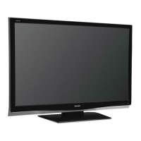
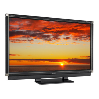
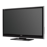
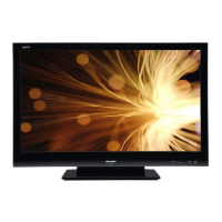
LC-42XL2E/S/RU, LC-46XL2E/S/RU, LC-46X20E/S/RU, LC-52XL2E/S/RU, LC-52X20E/S/RU
5 – 36
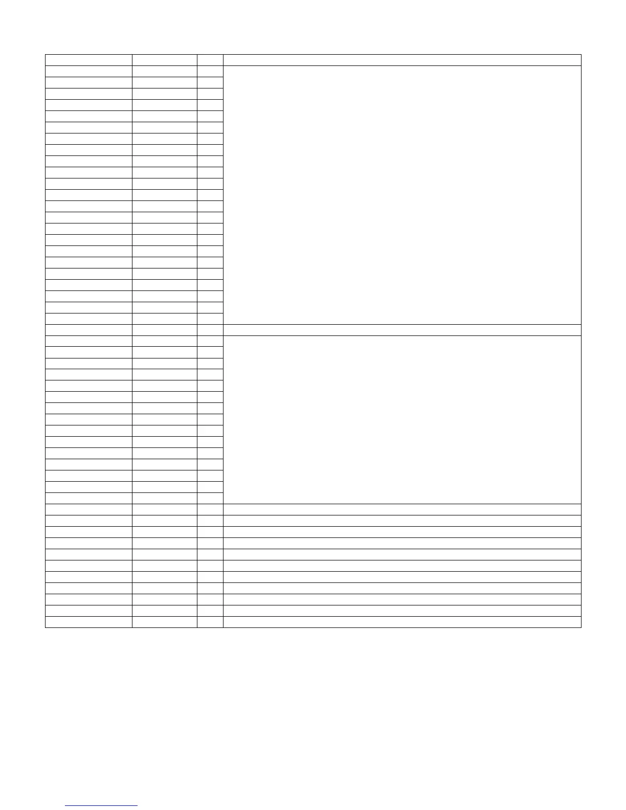
2.18.2 Pin Connections and short description
Pin No. Pin Name I/O Pin Function
2 A22 I 23 Address inputs
15 A21 I
12 A20 I
11 A19 I
18 A18 I
19 A17 I
54 A16 I
3A15I
4A14I
5A13I
6A12I
7A11I
8A10I
9A9I
10 A8 I
20 A7 I
21 A6 I
22 A5 I
23 A4 I
24 A3 I
25 A2 I
26 A1 I
31 A0 I
51 DQ15/A-1 I/O DQ15 (Data input/output, word mode), A-1(LSB Address input, byte mode)
49 DQ14 I/O 15 Data inputs/outputs
47 DQ13 I/O
45 DQ12 I/O
42 DQ11 I/O
40 DQ10 I/O
38 DQ9 I/O
36 DQ8 I/O
50 DQ7 I/O
48 DQ6 I/O
46 DQ5 I/O
44 DQ4 I/O
41 DQ3 I/O
39 DQ2 I/O
37 DQ1 I/O
35 DQ0 I/O
32 CE# I Chip Enable input
34 OE# I Output Enable input
13 WE# I Write Enable input
16 WP#/ACC I Hardware Write Protect input/Programming Acceleration input
14 RESET# I Hardware Reset Pin input
53 BYTE# I Selects 8-bit or 16-bit mode
17 RY/BY# O Ready/Busy output
43 VCC — 3.0 volt-only single power supply
29 VIO O Output Buffer power.
33, 52 VSS — Device Ground
1, 27, 28, 30, 55, 56 N.C — Pin not Connected Internally.