LC-42XL2E/S/RU, LC-46XL2E/S/RU, LC-46X20E/S/RU, LC-52XL2E/S/RU, LC-52X20E/S/RU
5 – 37
2.19. IC8702 (RH-iXC0150WJQZY)
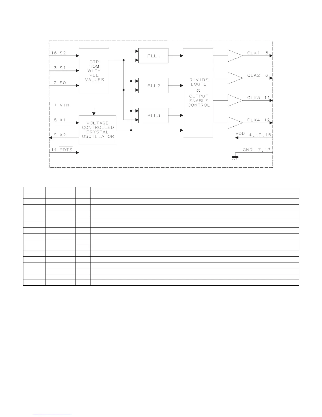
2.19.1 Block Diagram
2.19.2 Pin Connections and short description
Pin No. Pin Name I/O Pin Function
1 VIN I Voltage input to VCXO. Zero to 3.3V signal which controls the VCXO frequency.
2 S0 I Select pin 0. Internal pull-up resistor.
3 S1 I Select pin 1. Internal pull-up resistor.
4 VDD — Connect to +3.3 V.
5 CLK1 O Output clock 1. Weak internal pull-down when tri-state.
6 CLK2 O Output clock 2. Weak internal pull-down when tri-state.
7 GND — Connect to ground.
8 X1 I Crystal input. Connect this pin to a crystal.
9 X2 O Crystal Output. Connect this pin to a crystal.
10 VDD — Connect to +3.3 V.
11 CLK3 O Output clock 3. Weak internal pull-down when tri-state.
12 CLK4 O Output clock 4. Weak internal pull-down when tri-state.
13 GND — Connect to ground.
14 PDTS I Power-down tri-state. Powers down entire chip and tri-states clock outputs when low. Internal pull-up resistor.
15 VDD — Connect to +3.3 V.
16 S2 I Select pin 2. Internal pull-up resistor.