– 79 –
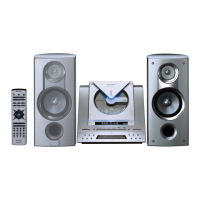
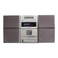
MD-E9000H
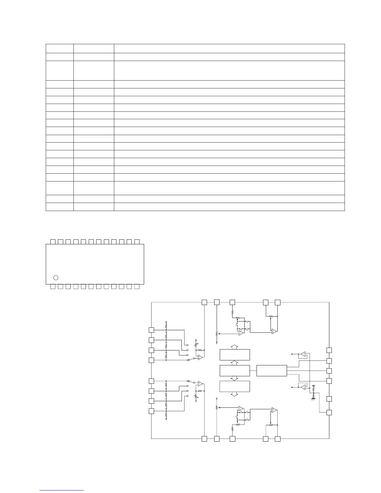
IC401 VHiLC75341/-1: Audio Processor (LC75341)
1 DI Serial data and clock input terminal for control.
2 CE Chip enable terminal.
When changing from "H" to "L", data is written in the internal latch and each analog switch is turned on.
Data transmission is enabled at "H" level.
3 VSS Ground terminal.
4 LOUT Bass band filter construction capacitor/resistor connection terminal and bass/treble output terminal.
5 LBASS Bass band filter capacitor and resistor connection terminal.
6 LTRE Treble band filter capacitor connection terminal.
7 LIN L-CH signal input terminal.
8 LSEL0 Input selector output terminal.
9-12 (10*) L4-L1 Input signal terminal.
13-16 (15*) R1-R4 Input signal terminal.
17 RSEL0 Input selector output terminal.
18 RIN R-CH signal input terminal.
19 RTRE Treble band filter capacitor connection terminal.
20 RBASS Bass band filter capacitor and resistor connection terminal.
21 ROUT Bass band filter capacitor/resistor connection terminal and bass/treble output terminal.
22 VREF 0.5 × VDD voltage generation section for analog ground. Connect a capacitor of 10 µF or more between
Vref and AVSS (VSS) as a countermeasure against the power supply ripple.
23 VDD Power supply terminal.
24 CLK Serial data and clock input terminal for control.
Pin No. Terminal Name
Function
In this unit, the terminal with asterisk mark (*) is (open) terminal which is not connected to the outside.
Figure 79 BLOCK DIAGRAM OF IC