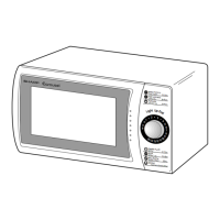
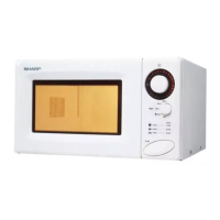
17
R-200BK
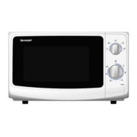
R-200BW
DESCRIPTION OF LSI
LSI(IZA860DR)
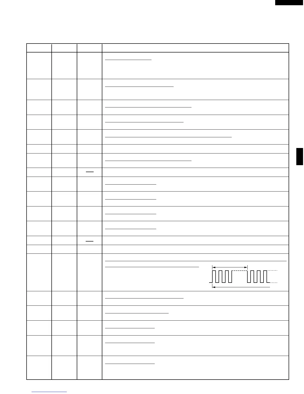
The I/O signal of the LSI(IZA860DR) are detailed in the following table.
Pin No. Signal I/O Description
16.7 msec.
During cooking
H
L
1 RST IN Auto clear terminal.
Signal is input to reset the LSI to the initial state when power is applied. Temporarily
set to “L” level the moment power is applied, at this time the LSI is reset. Thereafter
set at “H” level.
2 INT IN Signal coming from encoder.
When the encoder is turned, the contacts of encoder make pulse signals. And pulse
signals are input into INT.
3 AVSS IN A/D converter power source voltage.
The power source voltage to drive the A/D converter in the LSI. Connected to GND.
4 VREF IN Reference voltage input terminal.
A reference voltage is applied to the A/D converter in the LSI. Connected to GND.
5K0INTerminal to change functions according to the model.
Signal in accordance with the model in operation is applied to set up its function.
6 K1 IN Connected to GND.
7 AVDD IN A/D converter power source voltage.
The power source voltage to drive the A/D converter in the LSI.
8 NC No connection terminal.
9 S0 OUT Digit selection signal.
Signal is input to the anodes of the light-emitting diodes (LD1 - LD5).
10 S1 OUT Digit selection signal.
Signal is input to the anodes of the light-emitting diodes (LD6 - LD10).
11 S2 OUT Digit selection signal.
Signal is input to the anodes of the light-emitting diodes (LD11 - LD15).
12 S3 OUT Digit selection signal.
Signal is input to the anodes of the light-emitting diodes (LD16 - LD20).
13-14 NC No connection terminal.
15 D0 OUT Connected to VC.
16 D1 OUT Magnetron high-voltage circuit, oven lamp, turntable motor and fan motor
driving signal(Square Waveform : 60Hz)
To turn on and off the relay (RY1). In
100% POWER operation, the signals
hold “L” level during microwave cook-
ing and “H” level while not cooking.
17 CNVS IN Reference voltage input terminal.
A reference voltage is applied to the A/D converter in the LSI. Connected to GND.
18 VSS IN Power source voltage: -0V.
The power source voltage to drive the LSI is input to VSS terminal. Connected to GND.
19 D2 OUT Segment data signal.
Signal is input to the cathodes of the light-emitting diodes (LD1 ,LD6, LD11 and LD16).
20 D3 OUT Segment data signal.
Signal is input to the cathodes of the light-emitting diodes (LD1-LD2, LD6-LD7, LD12,
LD16 and LD17).
21 D4 OUT Segment data signal.
Signal is input to the cathodes of the light-emitting diodes (LD1-LD3, LD6-LD8, LD11-
LD13, LD16-LD17 and LD18).