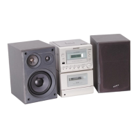
XL-505/505C,CP-505B
– 34 –
IC701 RH-iX0189AWZZ:System Microcomputer (IX0189AW) (1/2)
1-4 COM3-COM0 Output LCD COMMON output terminal
5-7 VLC3-VLC1 — LCD power terminal
8 VDD — Microcomputer power supply +5V.
9 OSC2 Output Main clock oscillator connection terminal f=8MHz
10 OSC1 Input Main clock oscillator connection terminal f=8MHz
11 VSS — Microcomputer power supply GND
12 XI Input Sub-clock oscillator connection terminal f=32.768kHz
13 XO Output Sub-clock oscillator connection terminal f=32.768kHz
14 MMOD Input Memory mode selection terminal
15 VREF- — Power supply for AD converter GND
16 KEY0 AN0/PA0 Input Destination detection input this terminal serves as an A/D input port.
When resetting is performed, the destination setting is detected based on the DC voltage.
17 KEY1 AN0/PA1 Input Operation key input, max. 8 keys
18 KEY2 AN0/PA2 Input Operation key input, max. 8 keys
19 KEY3 AN0/PA3 Input POWER key input detection
20* KEY4 AN0/PA4 Input Tuner signal meter (S meter) voltage input terminal
IX0189AW: Unused terminal (regular input port)
21 KEY5 AN0/PA5 Input Cassette tape erroneous erasing preventing lug detection input
H: Record inhibited L: Record enable
22 KEY6 AN0/PA6 Input Tape run/END detection input If pulse input is detected, it is judged that the tape is running.
23 KEY7 AN7/PA7 Input Cassette mechanism operation status detection input
H: Mechanism stop L: Mechanism in operation
24 VREF+ — A/D converter power supply +5V
25 TXD SBO0/P00 Output Terminal to output data to TUNER PLL IC
26 RXD SBI0/P01 Input Data input from TUNER PLL IC
27 SBT0/P02 Output TUNER PLL IC sync clock output
28 SBO1/P03 Output Terminal to output data to VOL IC
29 SBI1/P04 Output VOL IC chip enable output "L"=OFF "H"=ON
30 SBT1/P05 Output VOL IC sync clock output
31 DK/BZER P06 Output TUNER PLL IC enable output "L"=OFF "H"=ON
32 RST/P27 Input RESET signal input
33* RMOUT P10 — Unused terminal
34 P11 Output Power mute output "H"=MUTE OFF "L"=MUTE ON
35 TM2IO P12 Output Power amplifier operation control output
H: Amplifier operation ON L: Amplifier operation OFF
36 TM3IO P13 Output CD servo power circuit control output H: CD power ON L: CD power OFF
37 TM4IO P14 Input Function setting input Reset mode: H: 4-step selection L: 3-step selection
38 IRQ0 P20 Input Power failure detection input L: Change to HALT mode
39 SENS IRQ1/P21 Input Remote controller signal input
40* IRQ2 P22 Input RDS IC sync clock input
41 IRQ3 P23 Input Radio stereo broadcast reception detection input L: Stereo broadcast reception
42 IRQ4 P24 Input Broadcast reception status detection input L: Broadcast wave reception
43* P30 Input RDS signal reception status detection H: RDS not received L: RDS received
44* P31 Input Data input from RDS IC
45 P32 Output LC78623E RESET signal output
46 LED0 WE/P50 Output TC9284F chip enable terminal L: BUS terminal active
47 LED1 RE/P51 Output TC9284F data sync clock output
48 LED2 CS/P52 Output TUNER mute output "H"=MUTE ON "L"=MUTE OFF
49*
LED3/S51 A16/P53
Output IND LED control output (when SRS2 is on) H: LED goes out L: LED lights
50*
LED4/S50 A17/P54
Output IND LED control output (when SRS1 is on) H: LED goes out L: LED lights
51 SEG49 P60/A0 Output Cassette mechanism solenoid drive control output
52 SEG48 P61/A1 Output Cassette mechanism motor drive control output
FUNCTION TABLE OF IC
Pin No.
FunctionTerminal Name
Input/Output
In this unit, the terminal with asterisk mark (*) is (open) terminal which is not connected to the outside.