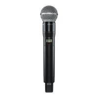
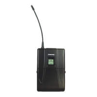
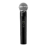
Shure T2 Vocal Artist Microphone Transmitter
2
Characteristics
25C1018 (CC)
Circuit Description
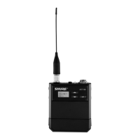
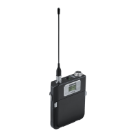
This unit contains two interconnected circuit boards that comprise
the audio and RF sections, respectively. It is intended for use with the
matching T3 and T4 receivers.
FCC-Approved vs. ETSI-Approved Models: Models approved by
the Federal Communications Commission (assembly number 90–8690,
with boards marked 34A8494) have different sections from those ap-
proved by the European Telecommunications Standards Institute (as-
sembly number 90–8705, with boards marked 34A8538). The FCC-ap-
proved version, sold in North America and many other places, uses only
the frequencies listed in Table 3 on page 12. The ETSI-approved version,
sold in Europe and many other places, uses only the frequencies listed
in Table 4 on page 13. Hence, the following circuit descriptions have sep-
arate sections for the two RF boards. The audio sections are the same
for all T2 models.
Audio Section
Input: The microphone element converts the sound source into an
electrical signal, which then enters the audio board through the center
contact of the head board (Figure 5, page 16).
Preamplifier Stage: This is centered in one section of operational
amplifier U102C. Externally accessible potentiometer R175 adjusts the
voltage gain of this stage over a 25 dB range.
Passive Pre-emphasis Network and Compandor: The network
(R145, C110, C111, C112, and R115) has a pole at 63 microseconds and
a zero at 12 microseconds. The NE571D integrated circuit compander
(U101A) provides 2:1 logarithmic compression of the audio signal.
Noise, Distortion, and Limiting: U102A lowers the noise floor, and
internal potentiometer R130 nulls the system audio distortion. Opera-
tional amplifier U102B, operating as a two-pole, active low-pass filter,
restricts the bandwidth of the system to the audio frequencies. PNP tran-
sistors Q103 and Q104 limit the level of the audio signal leaving the
audio section via U102B.
5 Vdc Bias and LED Drive Circuits: The NE571D’s identical second
channel (U101B) supplies regulated, low-noise 5 Vdc bias to various
audio and RF circuit points. Transistor Q105 provides “reverse battery
protection” to the circuit. Q106 drives LED D101 (“Power 0n”), and Q107
drives LED D102 (“Low Battery”).
RF Section: FCC-Approved Models
Audio Input: Processed audio enters R217, an internal potentiom-
eter that is adjusted for 15 kHz deviation (100% modulation) when the
audio section provides a –2.2 dBV, 1 kHz tone.
Oscillation: The audio then goes to varactor diode D201, which is
part of the modulated oscillator-tripler stage (Q201). The latter’s base-
emitter circuit operates as a crystal-controlled Colpitts oscillator in the
 Loading...