AN179
Rev. 0.4 7
6.3. Expansion I/O Connector (J1)
The
34
-pin Expansion I/O connector J1 provides access to all signal pins of the C8051F
31
0 device. Pins for +3 V,
digital ground and the output of an on-board low-pass filter are also available. A small through-hole prototyping area
is also provided. All I/O signals routed to connector J1 are also routed to through-hole connection points between J1
and the prototyping area (see
Figure 2 on page 5
). Each connection point is labeled indicating the signal available at
the connection point. See Table 2 for a list of pin descriptions for J1.
6.4. Target Board DEBUG Interface (J4)
The
DEBUG
connector (J4) provides access to the
DEBUG
(C2) pins of the C8051F310. It is used to connect the
Serial Adapter to the target board for in-circuit debugging and Flash programming. Table 3 shows the
DEBUG
pin
definitions.
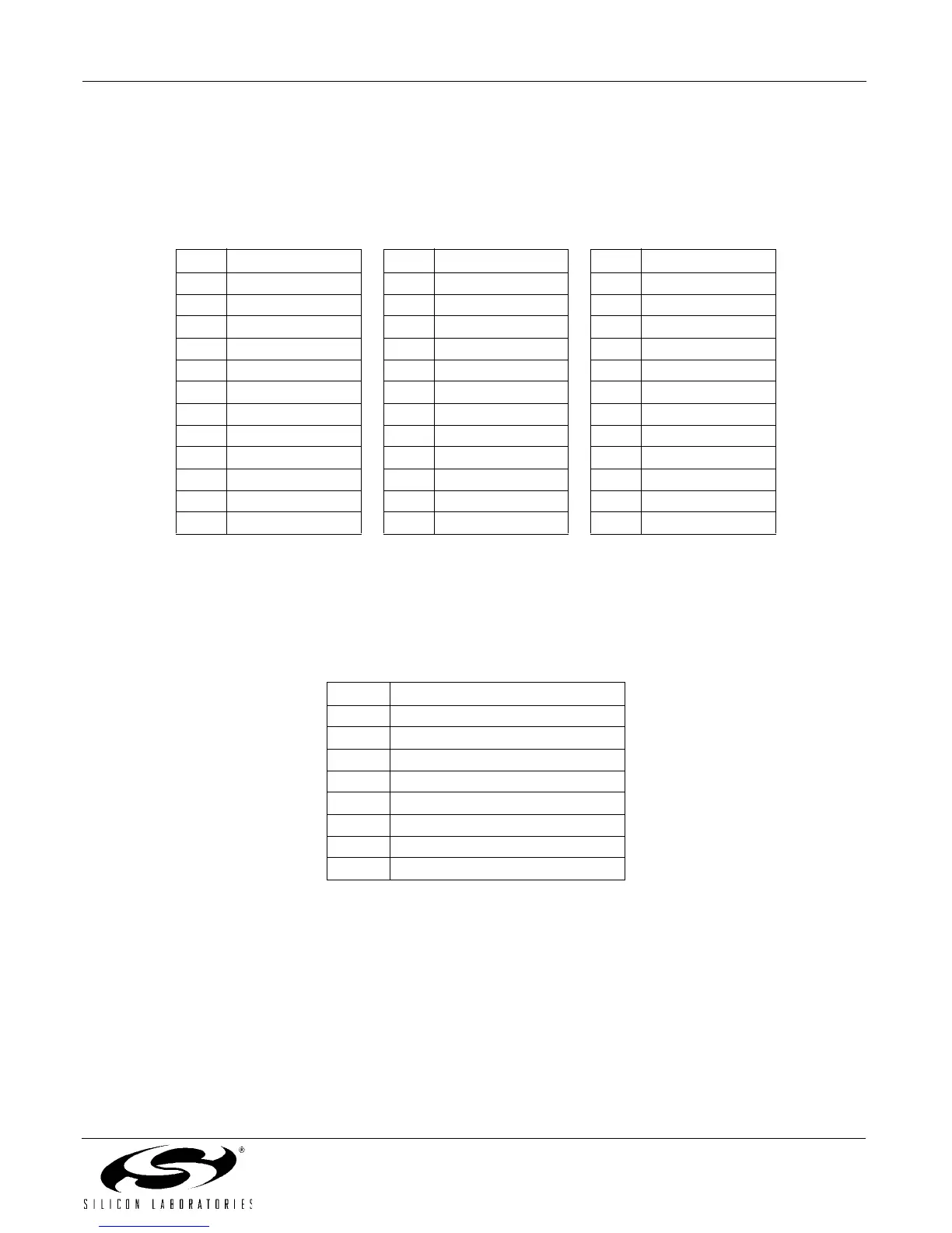
Pin # Description Pin # Description Pin # Description
1 +3VD (+3.3VDC) 13 P1.2 25 P2.6
2 PWM Output 14 P1.3 26 P2.7
3 P0.0 15 P1.4 27 P3.0
4 P0.1 16 P1.5 28 P3.1
5 P0.2 17 P1.6 29 P3.2
6 P0.3 18 P1.7 30 P3.3
7 P0.4 19 P2.0 31 P3.4
8 P0.5 20 P2.1 32 /RST (Reset)
9 P0.6 21 P2.2 33 GND (Ground)
10 P0.7 22 P2.3 34 GND (Ground)
11 P1.0 23 P2.4
12 P1.1 24 P2.5
Table 2. J1 Pin Descriptions
Pin # Description
1 +3VD (+3.3VDC)
2, 3, 9 GND (Ground)
4C2DAT
5/RST (Reset)
6P3.0
7C2CK
8 Not Connected
10 J4_Pin_10
Table 3. DEBUG Connector Pin Descriptions