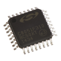
AN179
8 Rev. 0.4
6.5. Serial Interface (J5)
A RS232 transceiver circuit and DB-9 (J5) connector are provided on the target board to facilitate serial connec-
tions to UART0 of the C8051F310. The TX, RX, RTS and CTS signals of UART0 may be connected to the DB-9
connector and transceiver by installing shorting blocks on jumpers J3.
J3[5-6] - Install shorting block to connect UART0 TX (P0.4) to transceiver.
J3[7-8] - Install shorting block to connect UART0 RX (P0.5) to transceiver.
J3[9-10] - Install shorting block to connect UART0 RTS (P3.1) to transceiver.
J3[11-12] - Install shorting block to connect UART0 CTS (P3.2) to transceiver.
6.6. Analog I/O (J6)
Several of the C8051F310 target device’s port pins are connected to the J6 terminal block. Refer to Table 4 for the
J6 terminal block connections. Install a shorting block on J7[2-3] to connect the AIN2.4 input to the P2.4 pin of the
target device.
6.7. Serial Adapter Target Board Power Connector (J8)
The Serial Adapter includes a connection to provide power to the target board. This connection is routed from
J4[10] to J8[1]. Place a shorting block at jumper J8[2-3] to power the board directly from an AC/DC power adapter.
Place a shorting block at jumper J8[1-2] to power the board from the Serial Adapter. Please note that the second
option is not supported with either the EC1 or EC2 Serial Adapters.
6.8. Low-pass Filter (J7)
The C8051F310 target board features a low-pass filter that may be connected to port pin P2.4. Install a shorting
block on J7[1-2] to connect the P2.4 pin of the target device to the low-pass filter input. The output of the low-pass
filter is routed to the PWM signal at J1[2]. The C8051F310 may be programmed to generate a PWM (Pulse-Width
Modulated) waveform which is then input to the low-pass filter to implement a user-controlled PWM digital-to-ana-
log converter. Refer to Applications Note AN107 - Implementing 16-Bit PWM Using the PCA in the “documenta-
tion” directory on the CD-ROM for a discussion on generating a programmable DC voltage level with a PWM
waveform and low-pass filter.
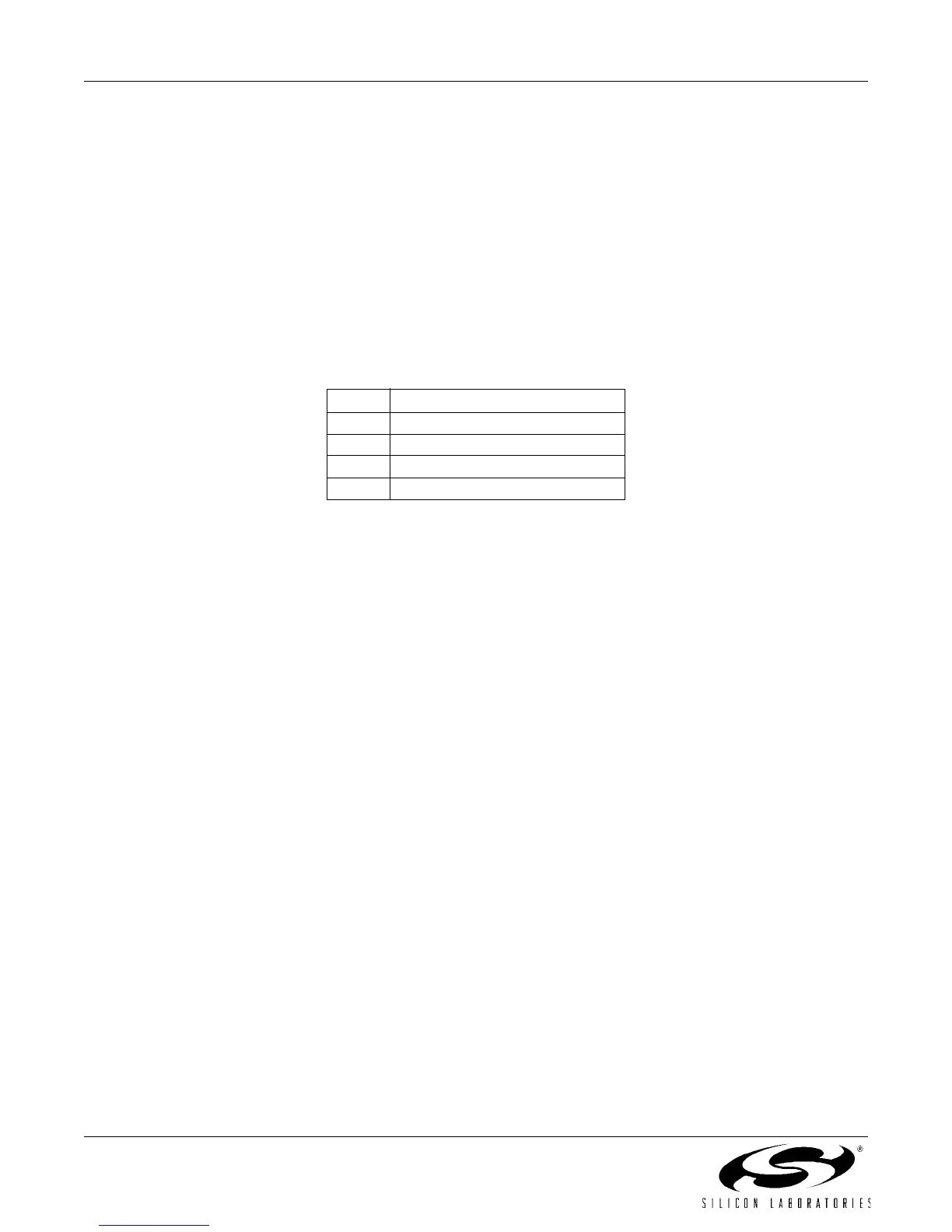
Pin # Description
1 P2.5 / AIN2.5
2AIN2.4
3 GND (Ground)
4 P0.0 / Vref (Voltage Reference)
Table 4. J6 Terminal Block Pin Descriptions