Do you have a question about the Silicon Laboratories Si5328 and is the answer not in the manual?
Details the Si5316 as a low jitter, precision jitter attenuator for high-speed communication systems.
Describes the Si5324 as a jitter-attenuating precision clock multiplier for applications requiring sub 1 ps jitter performance.
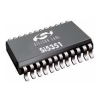
Describes the Si5328 as a jitter-attenuating precision clock multiplier for applications requiring sub-1 ps jitter performance.
Details the Si5374 as a highly integrated, 4-PLL jitter-attenuating precision clock multiplier.
Explains the clock multiplication circuit fundamental to the devices and the role of software tools.
Discusses PLL performance aspects including jitter generation and jitter transfer.
Defines jitter tolerance as the maximum input jitter before the DSPLL loses lock.
Explains internal self-calibration for optimizing loop parameters and jitter performance.
Describes clock selection capabilities: manual, auto, hitless, and revertive switching.
Explains holdover or VCO freeze mode, locking the DSPLL to a digital value.
Explains setting input frequency, multiplication ratio, and output frequency via register settings.
Explains the device performs internal self-calibration before operation.
Explains the device's holdover mode where the DSPLL is locked to a digital value.
Summarizes alarms indicating input signal status and frame alignment.
Explains the 2-wire bus for bidirectional communication using SDA and SCL lines.
Describes the 4-wire interface for microcontroller and serial peripheral communication.
Details differential inputs for CKINn clock inputs, bias voltage, and AC coupling.
Explains output clock configuration for compatibility with LVPECL, CML, LVDS, or CMOS.
Details interfaces for crystal or external clock references, including specific device limitations.
Details how the Si53xx reference source is determined by the device RATE[1:0] pin settings.
Explains f3 definition, its range, and its impact on jitter performance.
Recommends logically connecting RSTL_x pins for consistent reset behavior across DSPLLs.
| Brand | Silicon Laboratories |
|---|---|
| Model | Si5328 |
| Category | Computer Hardware |
| Language | English |