cDP.H3700
sEcfloN
4
DIAGRAMS
4.I. PIN DESCRIPTION
.
lC2Ol
GD System
Controller
(rPD75116GF-F21-3BE)
Functions
effected by the
captioned
controller
irrclude lCl0l
(RF
signal
processing,
sewo), IC202
(DSP,
digital filter)
and loading conrol in rhe
CD unit, data exchange with
IC4OI
(display
controller),
audio
bus entry,
etc.
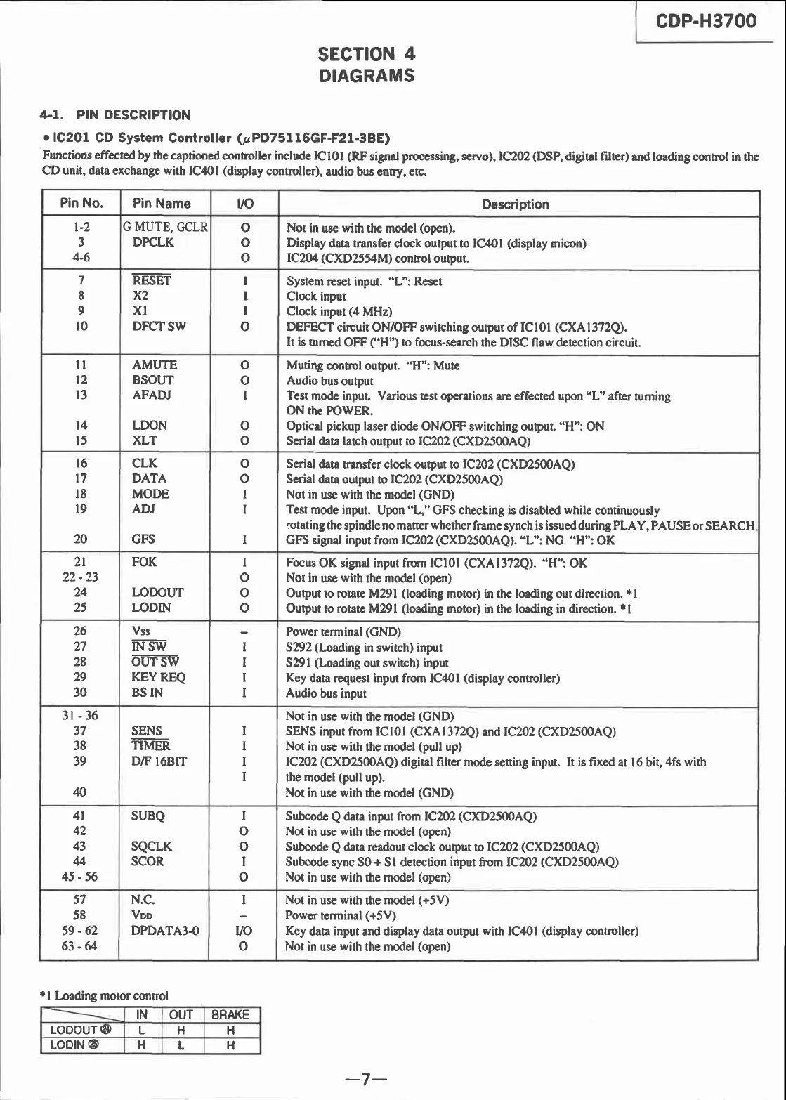
Pin No.
Pin
Name
vo Description
t-2
3
+6
G MUTE,
GCLR
DFCLK
o
o
o
Not in
usc
with
the model
(open).
Display
daa transfer
clock
output to IC4OI
(display
micon)
IC204
(CXD2554M)
connol ouçut.
7
8
9
t0
RBET
x2
xt
DFCTSW
I
I
I
o
System
rcset input.
"L":
Reset
Clock input
Clock
input
(4
MHz)
DEFECT
circuit ON/OFF switching
output of
ICl0l
(CXAI372Q).
It is
tumed
OFF
("H")
to focus-search
the DISC flaw detection circuit.
ll
t2
r3
l4
l5
AMUTE
BSOUT
AFADJ
LDON
XLT
o
o
I
o
o
Muting
control output.
"H": Muæ
Audio
bus ouput
Test
mode input.
Various
test operations
arc effected upon
"L"
after
turning
ON the
POWER.
Optical
pickup
laserdiodÊ
ONpFF switching output.
"H":
ON
Serial
data latch
output to
IC202
(CXD2500AQ)
t6
t7
IE
t9
20
CLK
DATA
MODE
ADJ
GFS
o
o
I
I
I
Serial
data
transfer clock output to
IC202
(CXD2500AQ)
Serial
data output to IC202
(CXD2500AQ)
Not in
use
with
the model
(CND)
Test
mode input.
Upon'L," GFS checking is
disabled
while
continuously
rctating
the spindle no matter
whetherframe
synch is issued during PLAY,
PAUSE
or SEARCH
GFS signal input
from
IC202
(CXD2500AQ).
"L":
NG
"H":
OK
2r
22-23
24
25
FOK
LODOUT
LODIN
I
o
o
o
Focus
OK signal input from IClOl
(CXAl372Q).
"H":
OK
Not in
use
with
the model
(open)
Ouput
to rotate M29l
(loading
motor)
in the loading out direction.
*l
Ouput
to rotate M29l
(loading
motor)
in the loading in direction.
rl
26
27
28
29
30
Vss
IW
oursw
KEYREQ
BS IN
I
I
I
I
Power
terminal
(GND)
5292
(Loading
in switch) input
S29l
(Loading
out swirch) input
Key
data rcquest input from IC4OI
Audio
bus input
(display
controller)
3l-36
37
38
39
N
SENS
Tiilm,
DÆ
I6BIT
I
I
I
I
Not in
use
with
the model
(GND)
SENS
input from ICl0l
(CXAI372Q)
and IC202
(CXD250AQ)
Not in
use
with
the
model
(pull
up)
IC202
(CXD2500AQ)
digital filter
mode
setting input. It is fixed
at 16 bit,4fs
with
the model
(pull
up).
Not in
usc
with
the model
(GND)
4l
42
43
4
45
-56
SUBQ
sQcLK
scoR
I
o
o
I
o
Subcode
Q
data input from IC202
(CXD2500AQ)
Not in
use
with
the model
(open)
Subcode
Q
data readout clock
ouput
tolC202
(CXD250AQ)
Subcodc
sync S0
+
Sl detection
input
from IC202
(CXD2500AQ)
Not
in use
with
the model
(open)
57
58
59-62
$-a
N.C.
Voo
DPDATA3.O
I
VO
o
Not
in
use
with
the
model
(+5V)
Power
terminal
(+5V)
Key
data
input
and display
data ouput with IC,tOl
(display
controller)
Not
in use
with
the model
(open)
*l
Loading motor control
IN
OUT BRAKE
LODOUT@
L H
H
LODIN
@
H
L H
-7-