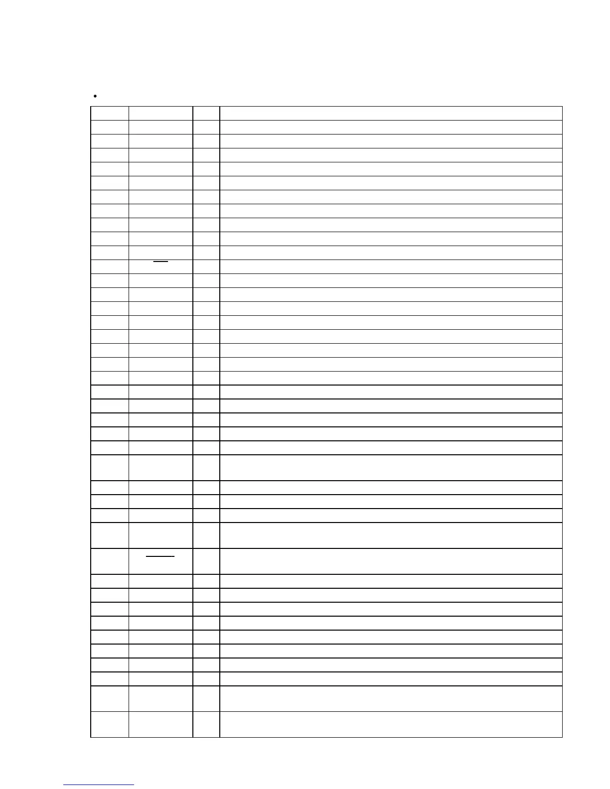
45
Pin No. Pin Name I/O Description
1A3O
Address signal output to the static RAM (IC202)
2A4O
Address signal output to the static RAM (IC202)
3A5O
Address signal output to the static RAM (IC202)
4A6O
Address signal output to the static RAM (IC202)
5A7O
Address signal output to the static RAM (IC202)
6A8O
Address signal output to the static RAM (IC202)
7A9O
Address signal output to the static RAM (IC202)
8 A10 O
Address signal output to the static RAM (IC202)
9 A11 O
Address signal output to the static RAM (IC202)
10 A12 O Address signal output to the static RAM (IC202)
11
WE O Write enable signal output to the static RAM (IC202)
12
NC O Not used (fixed at “H”)
13 NC O Not used (fixed at “H”)
14 LED-PLAY O N LED (D871) drive signal output terminal “H”: LED on
15 LED-PAUSE O
X LED (D872) drive signal output terminal “H”: LED on
16 LED-FILTER O FILTER LED (S886(2/2)) drive signal output terminal “H”: LED on
17 SPDL-MUTE O Mute signal output to the spindle motor driver (IC104, 105)
18 SHIFT-ON/OFF O
Reset signal output terminal Not used (open)
19 VOL UP O Volume up control signal output to the volume control motor driver (IC350)
20 VOL DOWN O Volume down control signal output to the volume control motor driver (IC350)
21
BLANK O Blank signal output to the fluorescent indicator tube driver (IC801 to IC803)
22
FL D0 O Serial data output to the fluorescent indicator tube driver (IC803)
23
FL D1 O Serial data output to the fluorescent indicator tube driver (IC802)
24
FL D2 O Serial data output to the fluorescent indicator tube driver (IC801)
25
FL CLK O Serial data transfer clock signal output to the fluorescent indicator tube driver (IC801 to IC803)
26
FL WR O Read/write select signal output to the fluorescent indicator tube driver (IC801 to IC803)
27 SENSER SW O
On/off control signal output to the stabilizer detect sensor (IC203) “H”: on
28 SENSER I Detect signal input from the stabilizer detect sensor (IC203) “H”: on
29
LIMIT OUT I
Detection input from the sled limit-out detect switch (S21)
The optical pick-up is outer position when “L”
30
RESET I
System reset signal input from the reset signal generator (IC204) “L”: reset
For several hundreds msec. after the power supply rises, “L” is input, then it changes to “H”
31
XTALI I Main system clock input terminal (4 MHz)
32
XTALO O Main system clock output terminal (4 MHz)
33
VSS — Ground terminal
34
TX O Sub system clock output terminal Not used (open)
35
TEX I Sub system clock input terminal Not used (fixed at “L”)
36
AVSS — Ground terminal (for A/D converter)
37
AVREF I Reference voltage input terminal (+5V)
38
K0 I Key input terminal (A/D input) ERASE key (S850) input
39
K1 I
Key input terminal (A/D input)
FILE, EDIT/TIME FADE, TIME, REPEAT, P MODE keys (S851 to S855) input
40 K2 I
Key input terminal (A/D input)
CHECK, CLEAR, FILTER, m, M , PUSH ENTER keys (S884 to S888, RV870) input
SERVO BOARD IC201 CXP84124-085Q (SYSTEM CONTROLLER)
 Loading...