46
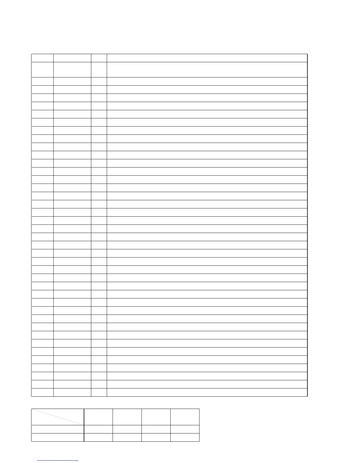
Pin No. Pin Name I/O Description
41 K3 I
Key input terminal (A/D input)
A OPEN/CLOSE, N, X, x keys (S889 to S892) input
42 K4 I Rotary encoder input terminal (A/D input) AMS L key (RV870) input
43 K5 I Rotary encoder input terminal (A/D input) AMS l key (RV870) input
44 ADJ/AFJ I Setting terminal for the test mode “L” active
45 IN/OUT SW I Detection input from the loading in/out detect switch (S281, S282) (A/D input)
46 SCLK O Sense serial data reading clock signal output to the CXD2545Q (IC101)
47 PRGL O Serial data latch pulse signal output to the CXD8762Q (IC600)
48 CLK O Serial data transfer clock signal output to the CXD2545Q (IC101) and CXD8762Q (IC600)
49 SENSE I Internal status (SENSE) signal input from the CXD2545Q (IC101)
50 DATA O Serial data output to the CXD2545Q (IC101) and CXD8762Q (IC600)
51 SQCK O Sub-code Q data reading clock signal output to the CXD2545Q (IC101)
52 SUBQ I Sub-code Q data signal input from the CXD2545Q (IC101)
53 TEST O Output terminal for the test Not used (open)
54 SEL1 I Destination setting terminal (fixed at “L”)
55 SEL0 I Destination setting terminal (fixed at “L”)
56 RMIN I Remote control signal input from the remote control receiver (IC804)
57 TIMER I Timer control input terminal Not used (fixed at “H”)
58 TEST O Output terminal for the test Not used (open)
59 TEST O Output terminal for the test Not used (open)
60 SCOR I Sub-code sync (S0+S1) detection signal input from the CXD2545Q (IC101)
61 AMUTE O Muting control signal output to the analog mute driver and mute relay driver
62 LDON O Laser diode on/off selection signal output to the RF amplifier in optical pick-up
63 XLT O Serial data latch pulse signal output to the CXD2545Q (IC101)
64 LOAD OUT O Loading motor (M271) drive signal output to the LB1641 (IC205) *1
65 LOAD IN O Loading motor (M271) drive signal output to the LB1641 (IC205) *1
66 DOUT O Digital out on/off control signal output terminal Not used (open)
67 DMUTE O Muting control signal output to the CXD2545Q (IC101) and CXD8762Q (IC600)
68 D0 I/O Two-way data bus with the static RAM (IC202)
69 D1 I/O Two-way data bus with the static RAM (IC202)
70 D2 I/O Two-way data bus with the static RAM (IC202)
71 D3 I/O Two-way data bus with the static RAM (IC202)
72 VDD — Power supply terminal (+5V)
73 NC I Not used (fixed at “H”)
74 D4 I/O Two-way data bus with the static RAM (IC202)
75 D5 I/O Two-way data bus with the static RAM (IC202)
76 D6 I/O Two-way data bus with the static RAM (IC202)
77 D7 I/O Two-way data bus with the static RAM (IC202)
78 A0 O Address signal output to the static RAM (IC202)
79 A1 O Address signal output to the static RAM (IC202)
80 A2 O Address signal output to the static RAM (IC202)
*1 Loading motor (M271) control
LOAD OUT (pin ^¢)
“L” “H” “L” “H”
LOAD IN (pin ^∞)
“L” “L” “H” “H”
OFF OUT IN BRAKE
Operatio


 To Next Page