2222
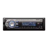
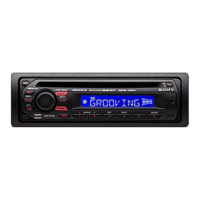
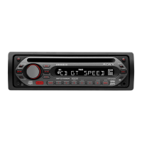
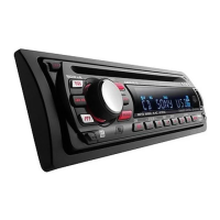
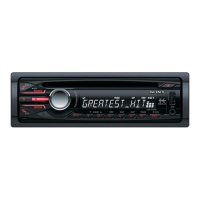
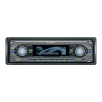
CDX-GT800D/GT805DX
CDX-GT800D/GT805DX
• NOTE FOR PRINTED WIRING BOARDS AND SCHEMATIC DIAGRAMS
THIS NOTE IS COMMON FOR PRINTED WIRING
BOARDS AND SCHEMATIC DIAGRAMS.
(In addition to this, the necessary note is
printed in each block.)
For schematic diagrams.
Note:
• All capacitors are in µF unless otherwise noted. (p: pF)
50 WV or less are not indicated except for electrolytics
and tantalums.
• All resistors are in Ω and
1
/
4
W or less unless otherwise
specified.
• f : internal component.
• C : panel designation.
For printed wiring boards.
Note:
• X : parts extracted from the component side.
• Y : parts extracted from the conductor side.
•
a
: Through hole.
• : Pattern from the side which enables seeing.
(The other layers' patterns are not indicated.)
• A : B+ Line.
• B : B– Line.
• H : adjustment for repair.
•Voltages and waveforms are dc with respect to ground
under no-signal (detuned) conditions.
• CD mechanism section (1/2), (2/2)
no mark : CD PLAY
• Main (1/4), (2/4), (3/4), (4/4) and Display sections
no mark : FM/MW/LW
<>: CD PLAY
∗
: Impossible to measure
•Voltages are taken with a VOM (Input impedance 10 MΩ).
Voltage variations may be noted due to normal production
tolerances.
•Waveforms are taken with a oscilloscope.
Voltage variations may be noted due to normal production
tolerances.
• Circled numbers refer to waveforms.
• Signal path.
J : CD PLAY
F : FM
f : MW/LW
L : BUS AUDIO
Caution:
Pattern face side: Parts on the pattern face side seen from the
(Side B) pattern face are indicated.
Par ts face side: Parts on the parts face side seen from the
(Side A) parts face are indicated.
Q
C
These are omitted
EB
E
These are omitted
CB
C
These are omitted
BE
• Waveforms
— SERVO Board —
(CD PLAY)
— MAIN Board —
Note: The components identified by mark 0 or dotted line
with mark 0 are critical for safety.
Replace only with part number specified.
4-4. CIRCUIT BOARDS LOCATION
MAIN board
SUB PANEL board
DISPLAY board
BASE PANEL board
SENSOR board
SERVO board
tuner unit
(TUX501
 Loading...