4
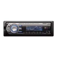
CDX-GT800D/GT805DX
TABLE OF CONTENTS
1. GENERAL
Location of Controls ........................................................ 5
Connections ..................................................................... 6
2. DISASSEMBLY
2-1. Base Panel Assy ............................................................... 10
2-2. Sub Panel Assy ................................................................ 10
2-3. CD Mechanism Block ..................................................... 11
2-4. Driving Section (DB-F05) ............................................... 11
2-5. Follow Move (F) Assy, Driving (F) Assy ........................ 12
2-6. Main Board ...................................................................... 12
2-7. Chassis (T) Sub Assy ....................................................... 13
2-8. Roller Arm Assy .............................................................. 13
2-9. Chassis (OP) Assy ........................................................... 14
2-10. Optical Pick-up ................................................................ 14
2-11. SL Motor Assy (M902) ................................................... 15
2-12. LE Motor Assy (M903) ................................................... 15
2-13. Servo Board ..................................................................... 16
3. DIAGNOSIS FUNCTION ........................................ 17
4. DIAGRAMS
4-1. Block Diagram –CD Section– ......................................... 19
4-2. Block Diagram –Main Section– ...................................... 20
4-3. Block Diagram –Display Section– .................................. 21
4-4. Circuit Boards Location .................................................. 22
4-5. Printed Wiring Boards –CD Mechanism Section– .......... 23
4-6. Schematic Diagram –CD Mechanism Section (1/2)– ..... 24
4-7. Schematic Diagram –CD Mechanism Section (2/2)– ..... 25
4-8. Printed Wiring Boards –Main Section– ........................... 26
4-9. Schematic Diagram –Main Section (1/4)– ...................... 28
4-10. Schematic Diagram –Main Section (2/4)– ...................... 29
4-11. Schematic Diagram –Main Section (3/4)– ...................... 30
4-12. Schematic Diagram –Main Section (4/4)– ...................... 31
4-13. Printed Wiring Boards –Panel Section– .......................... 32
4-14. Printed Wiring Board –Display Section– ........................ 33
4-15. Schematic Diagram –Display Section– ........................... 34
5. EXPLODED VIEWS
5-1. Main Section.................................................................... 46
5-2. Main Board Section ......................................................... 47
5-3. Front Panel Section ......................................................... 48
5-4. CD Mechanism Section (1) ............................................. 49
5-5. CD Mechanism Section (2) ............................................. 50
5-6. CD Mechanism Section (3) ............................................. 51
5-7. CD Mechanism Section (4) ............................................. 52
6. ELECTRICAL PARTS LIST .................................. 53
•
UNLEADED SOLDER
Boards requiring use of unleaded solder are printed with the lead-
free mark (LF) indicating the solder contains no lead.
(Caution: Some printed circuit boards may not come printed with
the lead free mark due to their particular size.)
: LEAD FREE MARK
Unleaded solder has the following characteristics.
• Unleaded solder melts at a temperature about 40°C higher than
ordinary solder.
Ordinary soldering irons can be used but the iron tip has to be
applied to the solder joint for a slightly longer time.
Soldering irons using a temperature regulator should be set to
about 350°C.
Caution: The printed pattern (copper foil) may peel away if the
heated tip is applied for too long, so be careful!
• Strong viscosity
Unleaded solder is more viscous (sticky, less prone to flow)
than ordinary solder so use caution not to let solder bridges
occur such as on IC pins, etc.
• Usable with ordinary solder
It is best to use only unleaded solder but unleaded solder may
also be added to ordinary solder.

 Loading...