– 31 – – 32 –
6-9. SCHEMATIC DIAGRAM — PRE SECTION — • Refer to page 48 for IC Block Diagrams.
Note on Schematic Diagram:
• All capacitors are in µF unless otherwise noted. pF: µµF
50 WV or less are not indicated except for electrolytics
and tantalums.
• All resistors are in Ω and
1
/
4
W or less unless otherwise
specified.
• C : panel designation.
• U : B+ Line.
• Power voltage is dc 9V and fed with regulated dc power
supply from battery terminal.
• Voltage and waveforms are dc with respect to ground
under no-signal (detuned) conditions.
no mark : FM
( ) : PB
< > : REC
[ ] : CD STOP
• Voltages are taken with a VOM (Input impedance 10 MΩ).
Voltage variations may be noted due to normal produc-
tion tolerances.
• Signal path.
F : FM
E : PB
a : REC
J : CD
Note on Printed Wiring Boards:
• X : parts extracted from the component side.
• b : Pattern from the side which enables seeing.
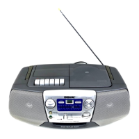
CFD-922L
(Page 35)
Q301
C
(REC)
• Waveform
1
4Vp-p
19.5µsec
5µsec/div
0.1V/div

 Loading...