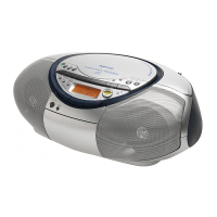
US,CND,E
MODEL
AR,SP
MODEL
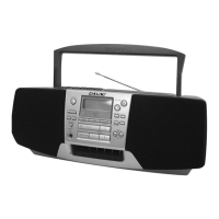
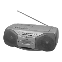
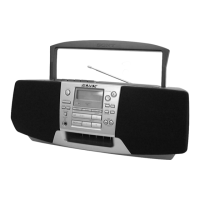
CFD-S38
– 29 – – 30 –
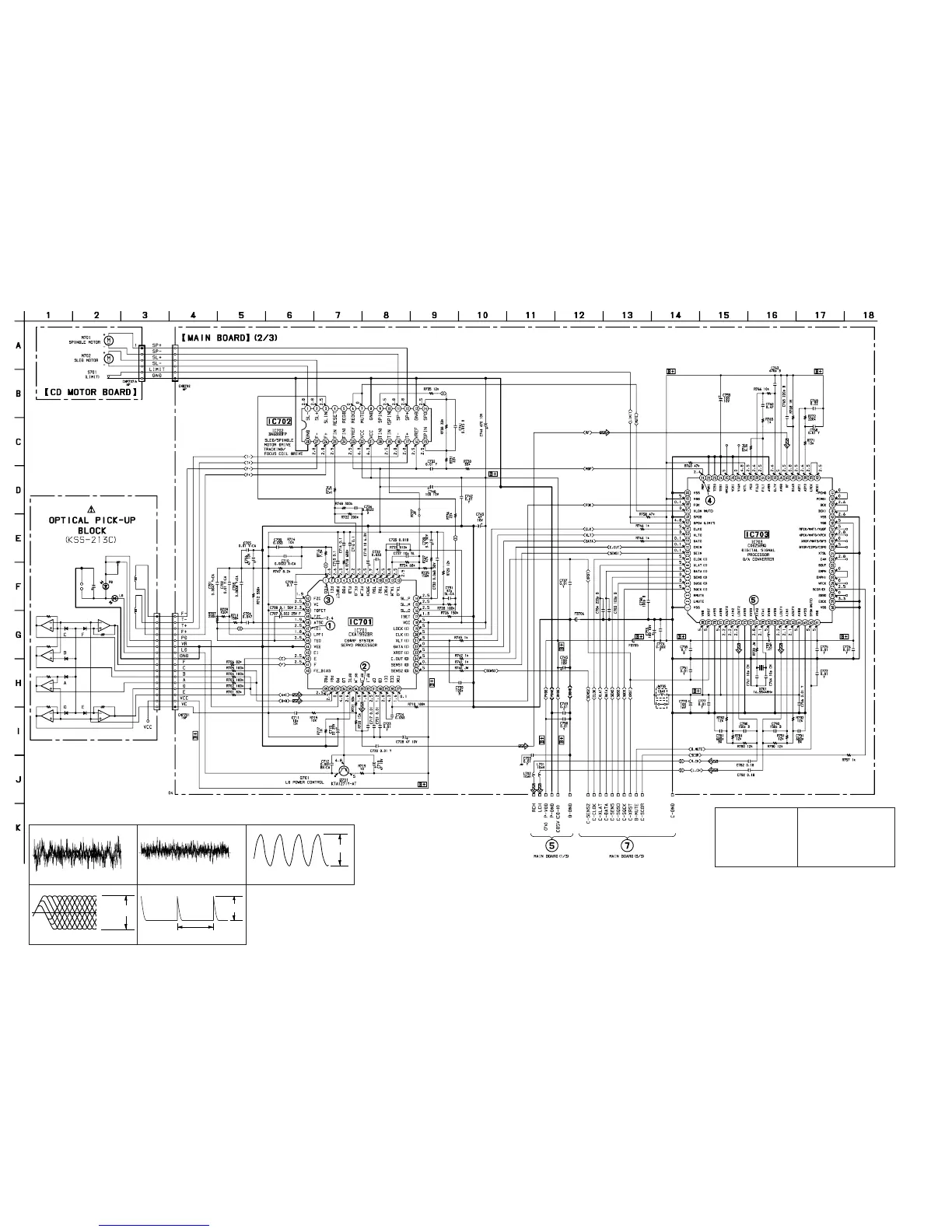
6-10. SCHEMATIC DIAGRAM — MAIN SECTION (2/3) — • Refer to page 38 for IC Block Diagrams.
Note:
• All capacitors are in µF unless otherwise noted. pF: µµF
50 WV or less are not indicated except for electrolytics
and tantalums.
• All resistors are in Ω and
1
/
4
W or less unless otherwise
specified.
• U : B+ Line.
• Power voltage is dc 9 V and fed with regulated dc power
supply from battery terminal.
• Voltage and waveforms are dc with respect to ground
under no-signal conditions.
no mark : CD STOP
• Voltages are taken with a VOM (Input impedance 10 MΩ).
Voltage variations may be noted due to normal produc-
tion tolerances.
• Waveforms are taken with a oscilloscope.
Voltage variations may be noted due to normal produc-
tion tolerances.
• Signal path.
J : CD
• Abbreviation
AR : Argentine model.
CND : Canadian model.
SP : Singapore model.
(Page 27)
(Page 31)
Note:
The components identi-
fied by mark ! or dotted
line with mark ! are criti-
cal for safety.
Replace only with part
number specified.
Note:
Les composants identifiés par
une marque ! sont critiques
pour la sécurité.
Ne les remplacer que par une
piéce portant le numéro
spécifié.
Approx. 100mVp-p
IC701
$
(TEI)
• Waveforms (MODE:PLAY)
1
2
3
4
5
2.5V
1.2±0.1Vp-p
Approx. 200mVp-p
IC701
1
(FEO)
2.5V
IC703
@¡
(MDP)
2Vp-p
7.6µsec
16.9344MHz
IC703
&¡
(XTAO)
2.2Vp-p
IC701
#£
(RFO)