– 14 –
D417 H-10
D418 H-10
D419 H-10
D420 H-10
IC101 F-7
IC201 D-7
IC301 E-9
IC302 G-10
Q101 F-11
Q201 F-10
Q301 G-7
Q302 H-9
Q303 C-8
Q304 C-8
Q305 F-10
Q306 D-8
Q307 G-9
Q401 H-11
Q402 H-11
D301 H-7
D302 G-7
D303 G-8
D304 D-8
D305 G-8
D306 G-7
D401 F-11
D402 G-11
D403 F-11
D404 F-11
D405 G-11
D406 F-11
D407 F-11
D408 G-11
D409 F-11
D410 F-11
D411 G-11
D412 F-11
D413 F-11
D414 G-11
D415 F-11
D416 H-10
Ref. No. Location
r
Semiconductor Location
Ref. No. Location
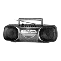
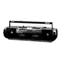
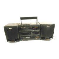
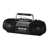
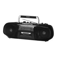
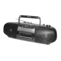
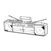
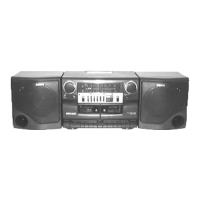
CFS-515S
Note on Printed Wiring Boards:
• X : parts extracted from the component side.
•
p : parts mounted on the conductor side.
• b : Pattern from the side which enables seeing.
Note on Schematic Diagram:
• All capacitors are in µF unless otherwise noted. pF: µµF
50 WV or less are not indicated except for electrolytics
and tantalums.
• All resistors are in Ω and
1
/
4
W or less unless otherwise
specified.
•
¢
: internal component.
• 2 : nonflammable resistor.
Note: The components identified by mark ! or dotted
line with mark ! are critical for safety.
Replace only with part number specified.
• U : B+ Line.
• H : adjustment for repair.
• Power voltage is dc 9V and fed with regulated dc power
supply from battery terminal.
• Voltages and waveforms are dc with respect to ground
under no-signal (detuned) conditions.
no mark : PLAY
( ) : REC
• Voltages are taken with a VOM (Input impedance 10 MΩ).
Voltage variations may be noted due to normal produc-
tion tolerances.
• Waveforms are taken with a oscilloscope.
Voltage variations may be noted due to normal produc-
tion tolerances.
• Circled numbers refer to waveforms.
• Signal path.
F : FM
E : PB (L-CH)
d : PB (R-CH)
a : REC (L-CH)
G : REC (R-CH)
r
Circuit Boards Location
POWER (AC) board
POWER (DC) board
BATT (+) board
BATT (–) board
TUNER board
REC SW board
MAIN board
VOL board
ECM board
 Loading...