– 20 – – 22 –– 21 –
r
Refer to page 24 for IC Block Diagram.
Ref. No. Location
r
Semiconductor
Location
D1 E-2
D2 E-2
D3 D-2
IC1 D-4
Q1 C-2
Q2 E-4
5-4. PRINTED WIRING BOARDS – TUNER SECTION –
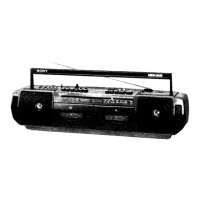
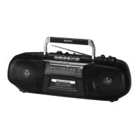
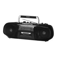
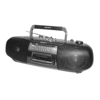
CFS-515S
5-5. SCHEMATIC DIAGRAM – TUNER SECTION –
Note:
• All capacitors are in µ F unless otherwise noted. pF: µµ F
50 WV or less are not indicated except for electrolytics
and tantalums.
• All resistors are in Ω and
1
/
4
W or less unless otherwise
specified.
•
¢
: internal component.
• U : B+ Line.
• H : adjustment for repair.
• Power voltage is dc 9V and fed with regulated dc power
supply from battery terminal.
• Voltages are dc with respect to ground under no-signal
(detuned) conditions.
no mark : FM
( ) : MW
< > : SW1,SW2
Note:
• X : parts extracted from the component side.
• b : Pattern from the side which enables seeing.
• Abbreviation
EA : Saudi Arabia
• Voltages are taken with a VOM (Input impedance 10 MΩ).
Voltage variations may be noted due to normal production
tolerances.
• Signal path.
F : FM
• Abbreviation
EA : Saudi Arabia
 Loading...