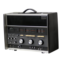
Section
Title
ourLINE
...........
3
l-1. Specifications
.......................................
3
l-2. Block Diagram
.......................................
5
l-3.
Technical
Features................................. 6
l-4. Circuit Explanations.............................. 6
l-5. External
View
.......................................10
l-6.
Internal
View..........................................10
l-7. Chassis View
..........................................11
DTSASSEMBLY
......................12
2-1. Rear Cover Removal.................,............ I 2
2-2.
Cabinet Removal
..........12
2-3. FrontPanel Removal
...........................13
2-4. Speaker Removal
..........13
2-5. Fm
Front
End
Removal........................14
2-6. A-m
I-f
Circuit Board Removal
.........14
2-7.
Fm I-f
Block Removal
........................15
2-8.
Cp Circuit Board Removal
.........'........16
2-g. Bfo Block Removal
..............................17
2-10. Sw Front End
Removal
........................17
2-ll.
Af. Circuit Board
Removal
..................18
2-12. Regulator Circuit Board Removal
.....18
2-13.
Power
Supply Circuit Board
Removal
.......................19
2-14.
DiaI Cord StringinC
.................. ............20
CIRCUIT ADJUSTMENTS
................. ..........22
3-1.
Preparation
...................22
3-2. A-m
I-fAlignment
..............................22
3-3.
Ssb Detector Adjustment
..............'.'.22
3-4.
Fm I-f
Alignment
..........23
3-5.
Muting Level Setting
...........................24
3-6.
FM l/FM2
Frequency Coverage
and Tracking Adjustment
..................24
3-7.
LWMWSWI Frequency
Coverage
and Tracking Adjustment
..................26
3-8.
SW2-SWl9 lst
I-f Alignment,
Frequency Coverage and
Tracking Adjustment
........................27
TABLE
OF
CONTENTS
Page
Section Title
Page
3-9.
SW2-SWl9 Frequency Coverage
and
Tracking
Adjustment
..................28
3-10.
Voltage
and Current Adjustment
......32
MOI.]NTING
AND SCHEMATIC
DTAGRAMS ............................33
4-1.
Bfo Block
(BFO-1A)
...........................33
4-2.
Jack Panel
......................34
4-3.
Antenna Terminal ..............................35
44.
Fm Front End Block
(FMC-l
38A
l
)
(
r
)
............ ...............36
4-5.
Fm Front End
Block
(FMC-
l 38A
I
)
(2)
............ ...............37
4-6.
SW2-SWl9
Front
End
Block
(swc-o1
lDl)
(l)
...........................38
4-7. SW2-SWI9
Front End Block
(swc-01
rDl)
(2)
...........................40
4-8.
FM
I-f
Block
(IF-5A)
.......................43
4-9.
Am I-f Circuit
Board
...........................45
4-10.
Cp
Circuit Board
.................................47
4-l l.
Regulator
Circuit
Board
......................49
4-12.
Power
Supply
Circuit Board
............50
4-13.
Af Circuit
Board
.................................51
4-14.
Schematic
Diagram
..............................
53
ELECTRJCAL
PARTS LIST
............ ............
s
7
E)fLODED
VIEW
AND
PACKING ,........66
6-1.
Hardware
Nomenclature
.....................66
6-2. Exploded View
(l)
.......................... ..
6'
6-3. Exploded View
(2)
..............................69
6-4. Exploded View
(3)
...........................
..-l
6-5. Exploded View
(4)
.........................
--:
6-6. Exploded View
(5)
.......................
...
-i
6-7. ExplodedView(6)
.............................
-t,
6-8.
Exploded
View
(7)
6-9.
Packing
...........................
-9
v
2-
J