tt
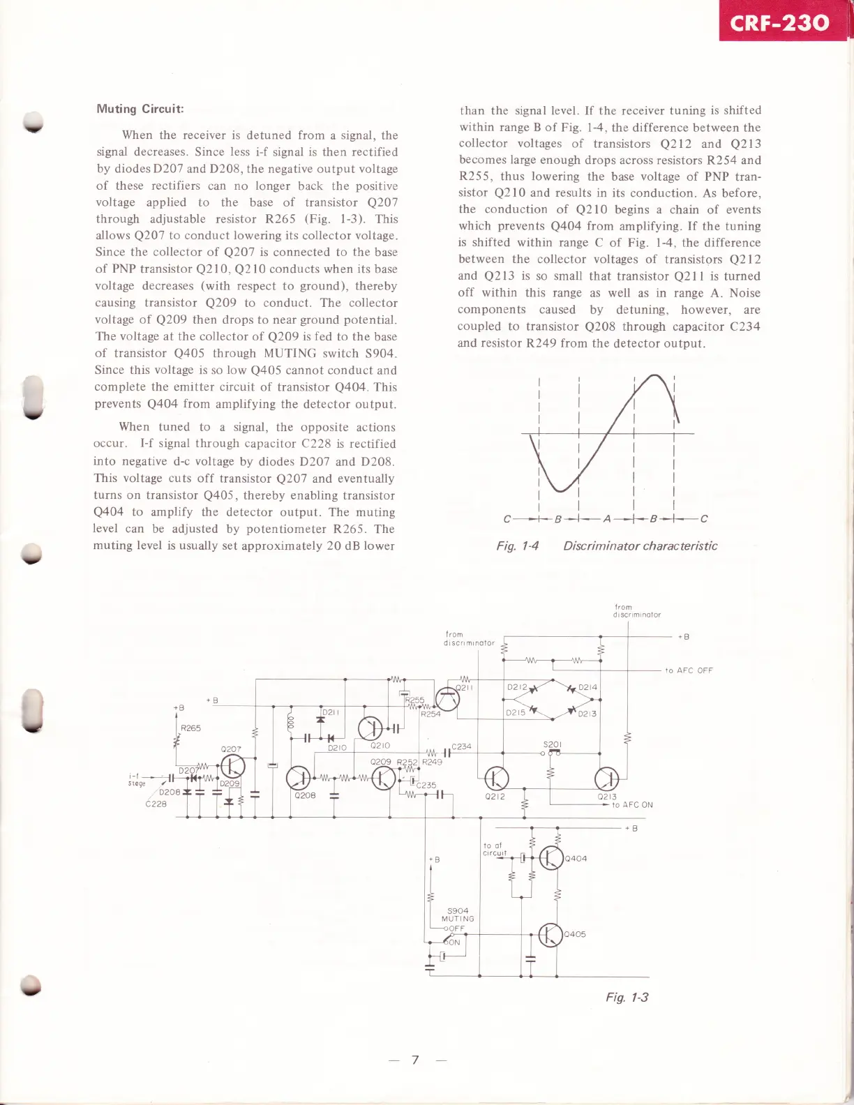
Muting Circuit:
When
the receiver is
detuned
from
a
signal,
the
signal
decreases. Since
less
i-f signal is then rectified
by diodes D2O7
and
D208,
the
negative
output
voltage
of these rectifiers
can
no longer
back the
positive
voltage
applied to the base of transistor
Q207
through adjustable resistor R265
(FiC.
l-3).
This
allows
Q207
to conduct lowering its
collector
voltage.
Since the
collector
of
Q207
is connected to the
base
of PNP
transistor
Q2
10,
Q2
l0 conducts when
its
base
voltage
decteases
(with
respect to
ground),
thereby
causing transistor
Q209
to conduct. The
collector
voltage of
Q209
then drops to near
ground
potential.
The
voltage at the collector
of
Q209
is
fed
to the
base
of
transistor
Q405
through MUTING switch
5904.
Since this
voltage
is so
low
Q405
cannot
conduct and
complete
the emitter circuit
of transistor
Q404.
This
prevents
Q404
from
amplifying
the detector output.
When tuned
to a signal,
the
opposite
actions
occur.
I-f
signal through capacitor
C228
is rectified
into
negative
d-c
voltage
by
diodes
D207
and
D208.
This voltage cuts
off
transistor
Q207
and eventually
turns on transistor
Q405,
thereby enabling transistor
Q404
to amplify
the detector output.
The
muting
level
can
be adjusted by
potentiometer
R265.
The
muting level is usually
set
approximately
20
dB
lower
than the
signal
level. If the receiver tuning
is shifted
within
range B of
Fig. 1-4,
the difference between the
collector
voltages
of
transistors
Q212
and
Q2l3
becomes large
enough
drops across resistors
R254
and
R255,
thus lowering
the base
voltage
of PNP
tran-
sistor
Q2
l0 and results in
its conduction.
As before,
the conduction
of
Q2
l0
begins
a chain
of events
which
prevents
Q404
from
amplifying. If the tuning
is shifted
within range
C of Fig. l-4, the difference
between
the collector voltages
of transistors
Q2
l2
and
Q2
13 is
so small that
transistor
Q2
l1
is
turned
off
within this range
as well as in range A. Noise
components
caused
by detuning, however, are
coupled
to transistor
Q208
through capacitor C234
and resistor
R249
from
the
detector
output.
C-f-a-f--
A-_-+-B-)--c
Fig. l-4 Discriminatorcharacteristic
!
v
trom
d
r
sc.rmr
notor
O2lA .27a
_
wlt--"
a209
R252 R249
9
7
Fig.
l-3


 To Next Page