EasyManua.ls Logo

Sony CX-JN5 User Manual

Sony CX-JN5
76 pages
To Next Page IconTo Next Page
Page #1 background imageLoading...
Page #1 background image
SERVICE MANUAL
Model Name Using Similar Mechanism NEW
CD Mechanism Type
CDM74-K6BD71A, CDM74S-K6BD71A,
CDM74S-K6BD72
CD
Base Unit Name BU-K6BD71A, BU-K6BD72
Section
Optical Block Name KSM-213DCP
Optical Pick-up Name KSS-213D
Tape deck
Model Name Using Similar Mechanism NEW
Section
Tape Transport Mechanism Type
CWM43FF13, CWM43FR16,
CWM43FR26
COMPACT DISC DECK RECEIVER
US Model
Canadian Model
AEP Model
UK Model
E Model
Australian Model
CX-JN5
Ver 1.2 2004.08
9-877-250-03 Sony Corporation
2004H05-1 Personal Audio Company
C 2004.08 Published by Sony Engineering Corporation
SPECIFICATIONS
CX-JN5 is the amplifier, CD player, tape deck
and tuner section in JAX-N5/PK5.
TUNER
FM tuning range
Except CIS model:
CIS model:
87.5 MHz to 108 MHz
FM usable sensitivity (IHF)
Except AEP, UK, CIS models:
AEP, UK models:
CIS model:
13.2
dBf
FM antenna terminal 75 ohms (unbalanced)
AM tuning range
US, CND, E51, MX models:
AEP, UK, CIS, E, SP, TW models:
KR, AUS models:
530 kHz to 1710 kHz (10 kHz step)
531 kHz to 1710 kHz (9 kHz step)
AM usable sensitivity 350 µV/m
AM antenna Loop antenna
AMPLIFIER
Power output
US, CND models:
96 W + 96 W (40 Hz - 20 kHz, THD
less than 1 %, 6 ohms)
120 W + 120 W (1 kHz, THD less
than 10 %, 6 ohms)
Total harmonic distortion
US, CND models:
AEP, UK, CIS models:
Except US, CND, AEP,
UK, CIS models:
0.08 % (45 W, 1 kHz, 6 ohms)
Input VIDEO/AUX: 400 mV
Outputs SPEAKERS: 6 ohms or more
PHONES: 32 ohms or more
CASSETTE DECK
T
rack format 4 tracks, 2 channels stereo
Frequency response 50 Hz – 8 kHz
GENERAL
Power requirements
US, CND, MX models:
AEP, UK, CIS models:
E, E51, SP, TW models:
KR model:
AUS model:
120 V AC, 60 Hz
65 MHz to 74 MHz (10 kHz step)
87.5 MHz to 108 MHz (50 kHz step)
15.3 dBf (65 MHz to 74 MHz)
12.8 dBf (87.5 MHz to 108 MHz)
531 kHz to 1602 kHz
0.08 % (32 W, 1 kHz, 6 ohms, DIN
AUDIO)
230 V AC, 50/60 Hz
16.8 dBf
531 kHz to 1602 kHz (9 kHz step)
530 kHz to 1710 kHz (10 kHz step)
0.08 % (40 W, 1 kHz, 6 ohms, DIN
AUDIO)
110 - 120 V/220 - 240 V AC
(switchable), 50/60 Hz
220 V AC, 60 Hz
240 V AC, 50/60 Hz
Rated: 64 W + 64 W (6 ohms, T.H.D.
1 %, 1 kHz/DIN 45500)
Reference: 80 W + 80 W (6 ohms,
T.H.D. 10 %, 1 kHz/DIN 45324)
MUSIC POWER: 195 W +195 W
AEP, UK, CIS models:
Rated: 80 W + 80 W (1 kHz, T.H.D.
1 %, 6 ohms )
Reference: 100 W + 100 W (1 kHz,
T.H.D. 10 %, 6 ohms)
Except US, CND, AEP,
UK, CIS models:
Recording system AC bias
Heads Deck A: playback x 1
Deck B: recording/playback x 1,
erase x 1
CD PLAYER
Laser Semiconductor laser (λ = 780 nm)
Emission duration:
continuous
D/A converter 1 bit dual
Signal-to-noise ratio 85 dB (1 kHz, 0 dB)
Harmonic distortion 0.05 % (1 kHz, 0 dB)
Power consumption
US, CND models:
AEP, UK, CIS models:
100 W
93 W
– Continued on next page –

Table of Contents

Question and Answer IconNeed help?

Do you have a question about the Sony CX-JN5 and is the answer not in the manual?

Sony CX-JN5 Specifications

General IconGeneral
BrandSony
ModelCX-JN5
CategoryStereo System
Speaker Configuration2-Way
CD PlayerYes
BluetoothNo
USB PortNo
Remote ControlYes
Cassette DeckYes
TunerAM/FM
Speakers2

Summary

Specifications Overview

Tuner Specifications

Details FM/AM tuning ranges, sensitivity, and antenna specifications.

Amplifier Specifications

Details power output specifications for different models.

CD Player Specifications

Details laser, D/A converter, S/N ratio, and distortion.

General Specifications

Details power requirements and consumption.

Safety Precautions and Handling

Safety Check-out Procedures

Outlines post-repair safety checks, including AC leakage testing.

Leakage Test Details

Specifies AC leakage limits and measurement methods.

Component Handling Precautions

Provides notes on chip component and flexible circuit board repair.

Critical Component Warning

Highlights critical components for safe operation and replacement advice.

Servicing Notes

Optical Pick-up and Laser Diode Handling

Instructions for safe handling of optical pick-up and laser diode.

Unleaded Solder and Model Identification

Information on unleaded solder and model identification.

Unit Controls and Connections

Front Unit Controls

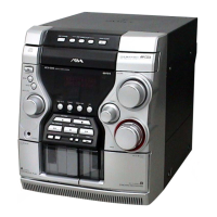
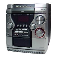
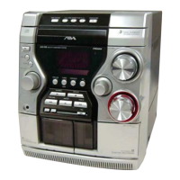
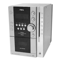
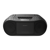
Identifies and describes the controls on the front panel of the main unit.

Rear Unit Connections

Identifies and describes the connections on the rear panel of the main unit.

Remote Control and Clock Settings

Remote Control Functions

Explains the functions of various buttons on the remote control.

Clock Setting Procedure

Provides instructions on how to set the unit's clock using the remote.

Disassembly Procedures

Disassembly Flowchart

Presents a visual flowchart detailing the sequence of disassembly steps.

Case Disassembly Steps

Side Case Removal

Details the procedure for removing the left and right side cases.

Top Case Removal

Details the procedure for removing the top case.

Internal Component Disassembly

Tray Panel Removal

Details the procedure for removing the tray panel.

CD Mechanism Deck Removal

Details the procedure for removing the CD mechanism deck.

Front Panel and Mechanical Deck Disassembly

Front Panel Section Removal

Details the procedure for removing the front panel section.

Mechanical Deck Removal

Details the procedure for removing the mechanical deck.

Chassis and Board Disassembly

Rear Cabinet Section Removal

Details the procedure for removing the rear cabinet section.

PT and Main Board Removal

Details the procedure for removing the PT and Main boards.

Test Mode Procedures

Reset and Test Modes

Covers Cold Reset, GC Test, and AMP Test modes.

Tray Lock and Repeat Mode

Details disc tray lock function and CD repeat limit cancel mode.

Electrical Adjustments and Checks

S-Curve and RF Level Checks

Details procedures for S-curve and RF level checks in the CD section.

System Diagrams

CD Section Block Diagram

Provides a block diagram illustrating the CD section's functional components.

Diagram Conventions and Locations

Notes on Diagramming

Explains conventions for PWB and schematic diagrams, including component identification.

Circuit Boards Location Map

Shows the physical locations of various circuit boards within the unit.

Printed Wiring Board Layouts

BD Section PWB (AEP, UK, CIS, E51, MX)

Shows the printed wiring board layout for the BD section for specific models.

BD Section Circuit Diagrams

BD Section Schematic (AEP, UK, CIS, E51, MX)

Provides the schematic diagram for the BD section for specific models.

BD Section Layouts

BD Section PWB (US, CND, E, SP, TW, KR, AUS)

Shows the printed wiring board layout for the BD section for other models.

BD Section Schematics

BD Section Schematic (US, CND, E, SP, TW, KR, AUS)

Provides the schematic diagram for the BD section for other models.

Changer Section Layouts

Changer Section PWBs

Shows the layout for the sensor, motor, SW, and driver boards.

Changer Section Schematics

Changer Section Schematic

Provides the schematic diagram for the changer section components.

Main Board Diagrams

Main Section Schematic (1/4)

First part of the main board schematic diagram.

Main Section Schematic (2/4)

Second part of the main board schematic diagram.

Main Section Schematic (3/4)

Third part of the main board schematic diagram.

Main Section Schematic (4/4)

Final part of the main board schematic diagram.

Main Board Layouts

Main Section Printed Wiring Board

Shows the component layout for the main board.

Headphone Section Diagrams

HP Section PWB Layout

Shows the component layout for the headphone section.

HP Section Schematic

Provides the schematic diagram for the headphone section.

Panel Section Layouts

Panel Section PWB Layout

Shows the component layout for the panel section.

Panel Section Schematics

Panel Section Schematic

Provides the schematic diagram for the panel section.

Key Section Layouts

Key Section PWBs

Shows the layout for the key and CD key boards.

Key Section Schematics

Key Section Schematic

Provides the schematic diagram for the key section.

PT Section Layouts

PT Section PWB (Except E, E51, SP, TW)

Shows the component layout for the PT section for specific models.

PT Section Schematics

PT Section Schematic (Except E, E51, SP, TW)

Provides the schematic diagram for the PT section for specific models.

PT Section Board Layouts

PT Section PWB (E, E51, SP, TW)

Shows the component layout for the PT section for other models.

PT Section Circuit Diagrams

PT Section Schematic (E, E51, SP, TW)

Provides the schematic diagram for the PT section for other models.

Waveforms and IC Diagrams

Waveform Measurements

Shows measured waveforms for various test points.

IC Block Diagrams

Illustrates block diagrams for key integrated circuits.

IC Pin Function Descriptions

Panel Board IC901 Pin Functions

Details the pin functions for the System Controller IC on the panel board.

IC Pin Function Details

Main Board IC Pin Functions

Details the pin functions for various ICs on the main board.

Exploded Views

Case Section Exploded View

Shows an exploded view of the unit's case components.

Front Panel Exploded Views

Front Panel Section-1 Exploded View

Shows an exploded view of the front panel components.

Front Panel Components

Front Panel Section-2 Exploded View

Shows another exploded view of front panel components.

Front Panel Details

Front Panel Section-3 Exploded View

Shows an exploded view of front panel parts like rings and keys.

Front Panel Assemblies

Front Panel Section-4 Exploded View

Shows an exploded view of front panel cabinets and springs.

Chassis and Power Components

Chassis Section Exploded View

Shows an exploded view of the chassis and power components.

CD Mechanism Deck Views

CD Mechanism Deck Section-1 Exploded View

Shows an exploded view of the CD mechanism deck parts.

CD Mechanism Parts Details

CD Mechanism Deck Section-2 Exploded View

Shows another exploded view of CD mechanism deck components.

CD Mechanism Assembly Views

CD Mechanism Deck Section-3 Exploded View

Shows an exploded view of CD mechanism deck assembly parts like pulleys and levers.

Base Unit Exploded Views

Base Unit Section Exploded View

Shows an exploded view of the base unit components.

Electrical Parts List

BD Section Capacitor List

Lists capacitors used in the BD section.

BD Section Component Lists

BD ICs, Transistors, and Resistors

Lists ICs, transistors, and resistors for the BD section.

BD Section Capacitors (Continued)

Continues the list of capacitors for the BD section.

Board Specific Parts Lists

BD, CD Key, Driver Components

Lists parts for BD, CD Key, and Driver sections.

Component Lists by Section

Driver, Headphone, Key Components

Lists parts for Driver, Headphone, and Key sections.

Panel Section Component Lists

Panel Connectors, Diodes, Shorts, LEDs, Transistors

Lists connectors, diodes, shorts, LEDs, and transistors for the panel section.

Main Section Component Lists

Main Switches, Resistors, Capacitors

Lists switches, resistors, and capacitors for the main section.

Main Section Component Details

Main Section Capacitors (Continued)

Continues the list of capacitors for the main section.

Main Section Component Data

Main Connectors, Diodes, Relay, Switch, Thermistor

Lists connectors, diodes, relays, switches, and thermistors for the main section.

Main ICs and Miscellaneous

Lists ICs, miscellaneous items, and accessories.

Panel Section Component Data

Panel Connectors, Diodes, Shorts, ICs, Transistors

Lists connectors, diodes, shorts, ICs, and transistors for the panel section.

Panel Section Resistors

Panel Resistors (Continued)

Continues the list of resistors for the panel section.

Main Section Resistors

Main Resistors (Continued)

Continues the list of resistors for the main section.

Main Section Resistor Details

Main Resistors (Continued)

Continues the list of resistors for the main section.

Main Section Resistor Information

Main Resistors (Continued)

Continues the list of resistors for the main section.

Board Specific Component Lists

Panel Connectors and Capacitors

Lists connectors and capacitors for the panel section.

Panel Section Component Data

Panel Indicator Tube, ICs, Shorts, Diodes, Transistors

Lists indicator tube, ICs, shorts, diodes, and transistors for the panel section.

Panel Section Resistor Data

Panel Resistors (Continued)

Continues the list of resistors for the panel section.

Panel and PT Section Components

Panel Vibrator, Capacitors, Connectors, Diodes

Lists vibrator, capacitors, connectors, and diodes for the panel section.

PT, Sensor, and Switch Section Components

PT Transformers, Relay, Switch, Connectors, ICs

Lists transformers, relay, switch, connectors, and ICs for the PT section.

Miscellaneous and Accessories

Lists miscellaneous items and accessories.

Related product manuals