32
CX-LEM550
• IC Pin Function Description
• CONTROL BOARD IC801 LC876980B-52T4-E (SYSTEM CONTROLLER)
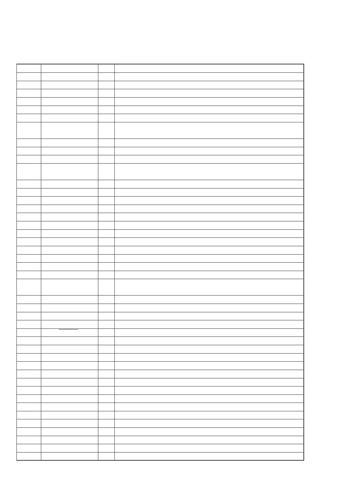
Pin No. Pin Name I/O Description
1 MI-ACK I Acknowledge signal input from the MP3 decoder
2 MP3-RST O Reset signal output to the MP3 decoder
3 MP3-REQ I Request signal input from the MP3 decoder
4MI-CS O Chip select signal output to the MP3 decoder
5 MI-LP O Serial data latch pulse output to the MP3 decoder
6 MP3-STB O Standby control signal output to the MP3 decoder
7 XTCN O
Oscillation circuit control signal output to the CD DSP
“H”: auto oscillation, “L”: oscillation off
8 X-RST O Reset signal output to the CD DSP
9XLT O Serial data latch pulse output to the CD DSP
10 SCOR I Subcode sync (S0+S1) detection signal input from the CD DSP
11 RESET I
Reset signal input from the reset switch “L”: reset For several hundreds msec.
after the power supply rises, “L” is input, then it changes to “H”
12 I-XT1 I Sub system clock input terminal (32.768 kHz)
13 O-XT2 O Sub system clock output terminal (32.768 kHz)
14 VSS1 — Ground terminal
15 XIN I Main system clock input terminal (10 MHz)
16 XOUT O Main system clock output terminal (10 MHz)
17 VDD1 — Power supply terminal (+3.2V)
18 I-POWER_MONITOR I Power monitor input terminal
19 MODEL DETECT I Model destination setting terminal
20 KEY1 I Front panel key input terminal (A/D input)
21 AREA I Model destination setting terminal
22 VOL_ENCODER I Dial pulse input of the rotary encoder (for VOLUME control)
23 I_POWER_DOWN I Power down detection signal input terminal “L”: power down, normally : “H”
24 TA-SW I
Cassette in/out detect switch signal input from the tape mechanism deck
“L”: cassette in
25 RDS-DATA I RDS serial data input from the FM/AM tuner unit
26 RDS-CLK I RDS serial data transfer clock signal input from the FM/AM tuner unit
27 KEY0 I Front panel key input terminal (A/D input)
28 F-DATA O Serial data output to the electrical volume
29 RMC_IN I Remote control signal input from the remote control receiver
30 NC VREF — Not used
31 to 42 G1 to G12 O Grid drive signal output to the fluorescent indicator tube
43 to 45 S1 to S3 O Segment drive signal output to the fluorescent indicator tube
46 VDD3 — Power supply terminal (+3.1V)
47 to 50 S4 to S7 O Segment drive signal output to the fluorescent indicator tube
51 VP — Power supply terminal (–29V)
52 to 60 S8 to S16 O Segment drive signal output to the fluorescent indicator tube
61 to 65 NC — Not used
66 CD OPEN I CD lid open/close detection switch input terminal
67 TA END SW I END switch signal input from the tape mechanism deck
68 TA PLAY SW I PLAY switch signal input from the tape mechanism deck
69 NC — Not used
70 TU STEREO I FM stereo detection signal input from the FM/AM tuner unit
71 TU TUNED I Tuning detection signal input from the FM/AM tuner unit
72 VDD4 — Power supply terminal (+3.1V)


 To Next Page