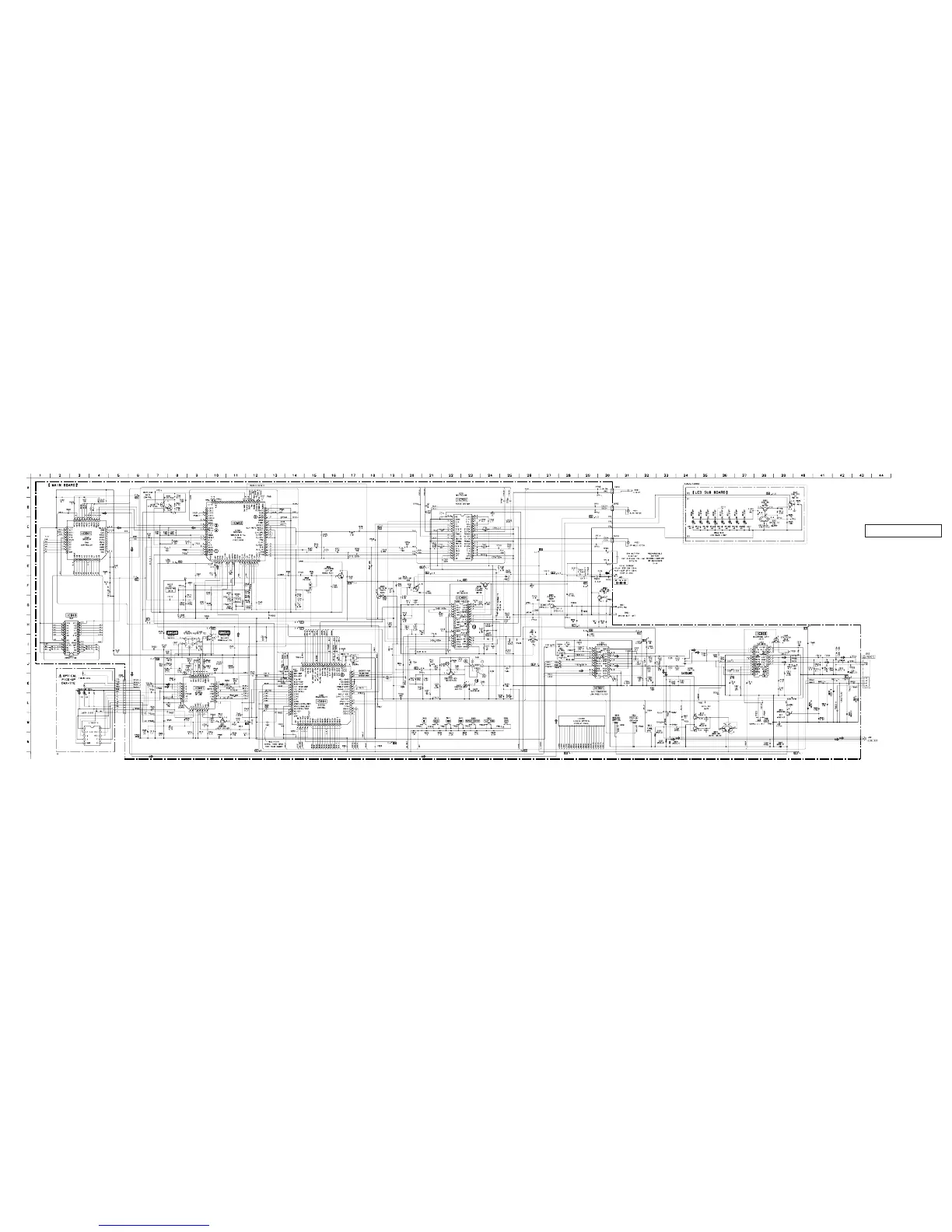
6-4. SCHEMATIC DIAGRAM
– 19 – – 20 – – 22 –– 21 – – 23 –
r
Refer to page 25 for IC Block Diagrams.
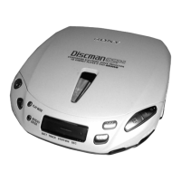
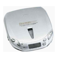
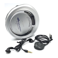
D-E451/E455/E456CK/E459CK
Note:
• All capacitors are in µF unless otherwise noted. pF: µµF
50 WV or less are not indicated except for electrolytics
and tantalums.
• All resistors are in Ω and
1
/
4
W or less unless otherwise
specified.
•
¢
: internal component.
Note: The components identified by mark ! or dotted
line with mark ! are critical for safety.
Replace only with part number specified.
• U : B+ Line.
• H : adjustment for repair.
• Power voltage is dc 4.5 V and fed with regulated dc power
supply from external power voltage jack. (J401)
• Voltages and waveforms are dc with respect to ground
under no-signal conditions.
• Voltages and current are taken with a VOM (Input imped-
ance 10 MΩ).
Voltage variations may be noted due to normal produc-
tion tolerances.
• Waveforms are taken with a oscilloscope.
Voltage variations may be noted due to normal produc-
tion tolerances.
• Circled numbers refer to waveforms.
• Signal path.
J : CD
r
Refer to page 24 for Waveforms.