○○○○○○○○○○○○○○○○○○○○○○○○○○○○○○○○○○○○○○○○○○○○○○○○○○○○○○○○○○○○○○○○○○○○○○○○○○○○○○○○○○○○○○○○○○○○○○○○○○○○○○○○○○
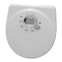
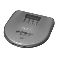
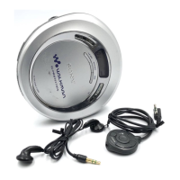
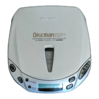
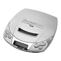
D-E770/EJ711/EJ715
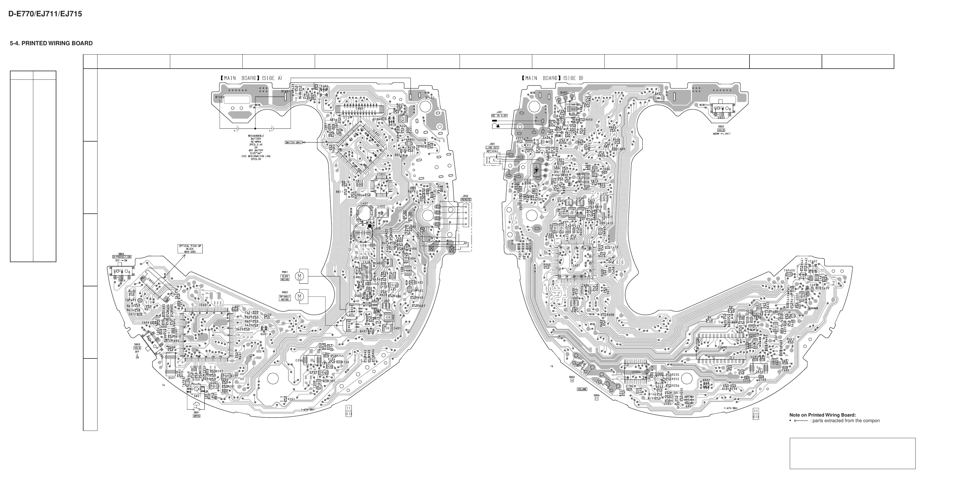
5-4. PRINTED WIRING BOARD
Note on Printed Wiring Board:
• X : parts extracted from the component side.
• Y : parts extracted from the conductor side.
• b : Pattern from the side which enables seeing.
Caution:
Pattern face side: Parts on the pattern face side seen from
(SIDE B) the pattern face are indicated.
Parts face side: Parts on the parts face side seen from
(SIDE A) the parts face are indicated.
Ref. No. Location
D401 A-8
D404 A-7
D406 C-5
D409 A-5
D410 C-4
D461 C-10
D601 D-3
IC301 E-8
IC351 E-8
IC401 C-7
IC402 C-10
IC404 A-4
IC601 D-2
IC602 D-9
IC801 B-4
IC802 B-4
Q301 E-9
Q302 E-9
Q401 A-7
Q402 A-7
Q403 A-7
Q404 A-7
Q405 D-4
Q406 D-4
Q407 D-4
Q408 D-4
Q412 A-7
Q413 A-5
Q501 C-10
Q601 A-5
• Semiconductor
Location
12
A
B
C
D
E
34567891011
— 12 — — 13 — — 14 —