D-E770/EJ711/EJ715
— 15 — — 16 — — 17 —
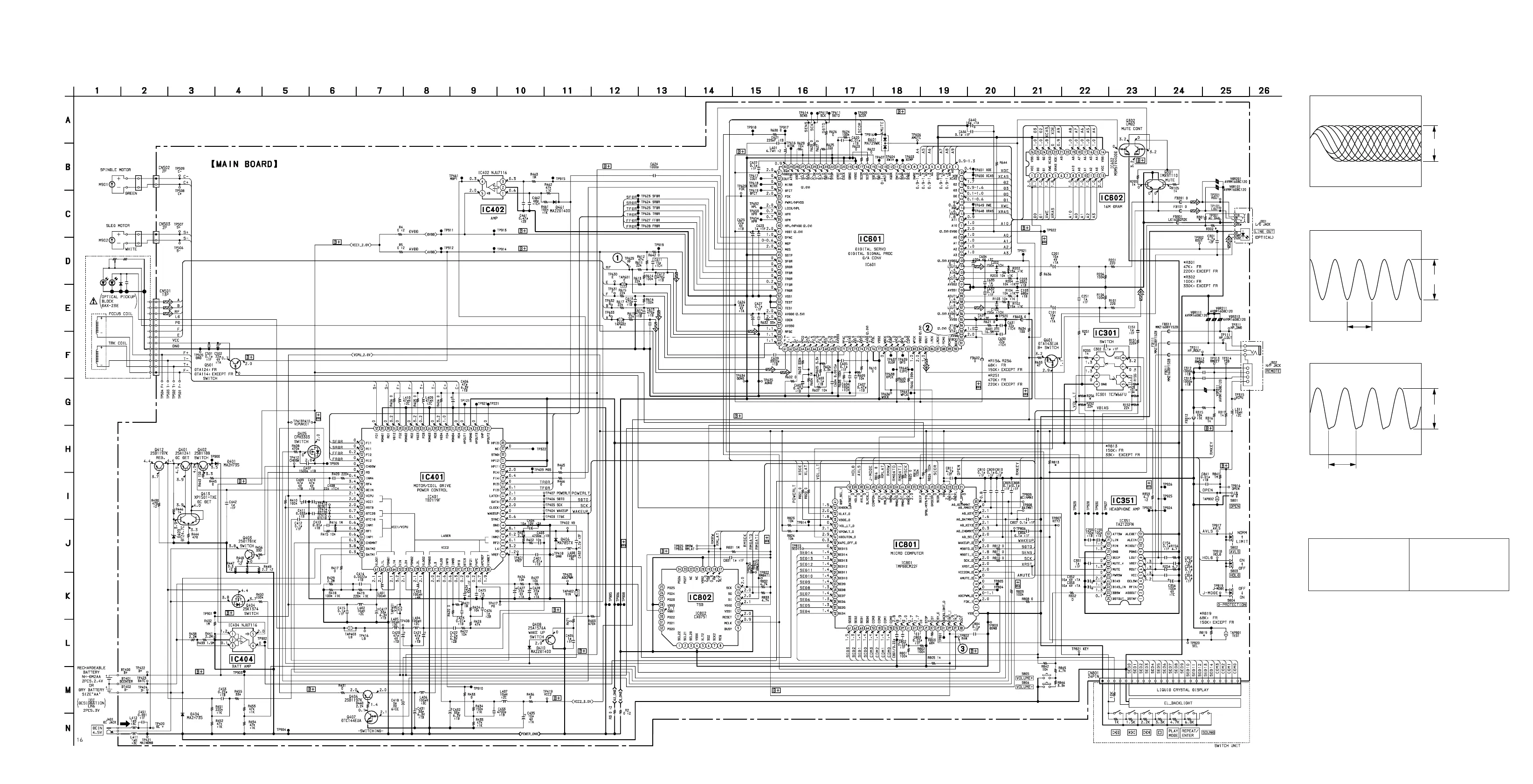
5-5. SCHEMATIC DIAGRAM
• Waveforms
Note on Schematic Diagram:
• All capacitors are in µF unless otherwise noted. pF: µµF
50 WV or less are not indicated except for electrolytics
and tantalums.
• All resistors are in Ω and
1
/
4
W or less unless otherwise
specified.
• U : B+ Line.
• Power voltage is dc 4.5 V and fed with regulated dc power
supply from external power voltage jack.
• Voltages and waveforms are dc with respect to ground
under conditions in service mode.
no mark : CD PLAY
• Voltages are taken with a VOM (Input impedance 10 MΩ).
Voltage variations may be noted due to normal produc-
tion tolerances.
• Waveforms are taken with a oscilloscope.
Voltage variations may be noted due to normal produc-
tion tolerances.
• Circled numbers refer to waveforms.
• Signal path.
J : CD PLAY (ANALOG OUT)
c : CD PLAY (OPTICAL OUT)
• Abbreviation
FR : French model
Note :
The components identified by
mark 0 or dotted line with mark
0 are critical for safety.
Replace only with part number
specified.
Note :
Les composants identifiés par
une marque 0 sont critiques
pour la sécurité.
Ne les remplacer que par une
pièce portant le numéro spécifié.
1 TP629 (RF) (PLAY MODE)
100 mV/DIV, 200 ns/DIV
2 IC601 od (XTAI)
500 mV/DIV, 20 ns/DIV
3 TP802 (R4M)
1 V/DIV, 100 ns/DIV
350 – 650 mVp-p
2.1 Vp-p
58.8 ns
3.4 Vp-p
237 ns
• Refer to page 9 for IC Block Diagrams. • Refer to page 7 for IC Pin Function Description.
• TOTAL CURRENT
PLAY : 160mA
STOP : 50mA
FF : 170mA
FR : 170mA
CXD3027R