— 7 —
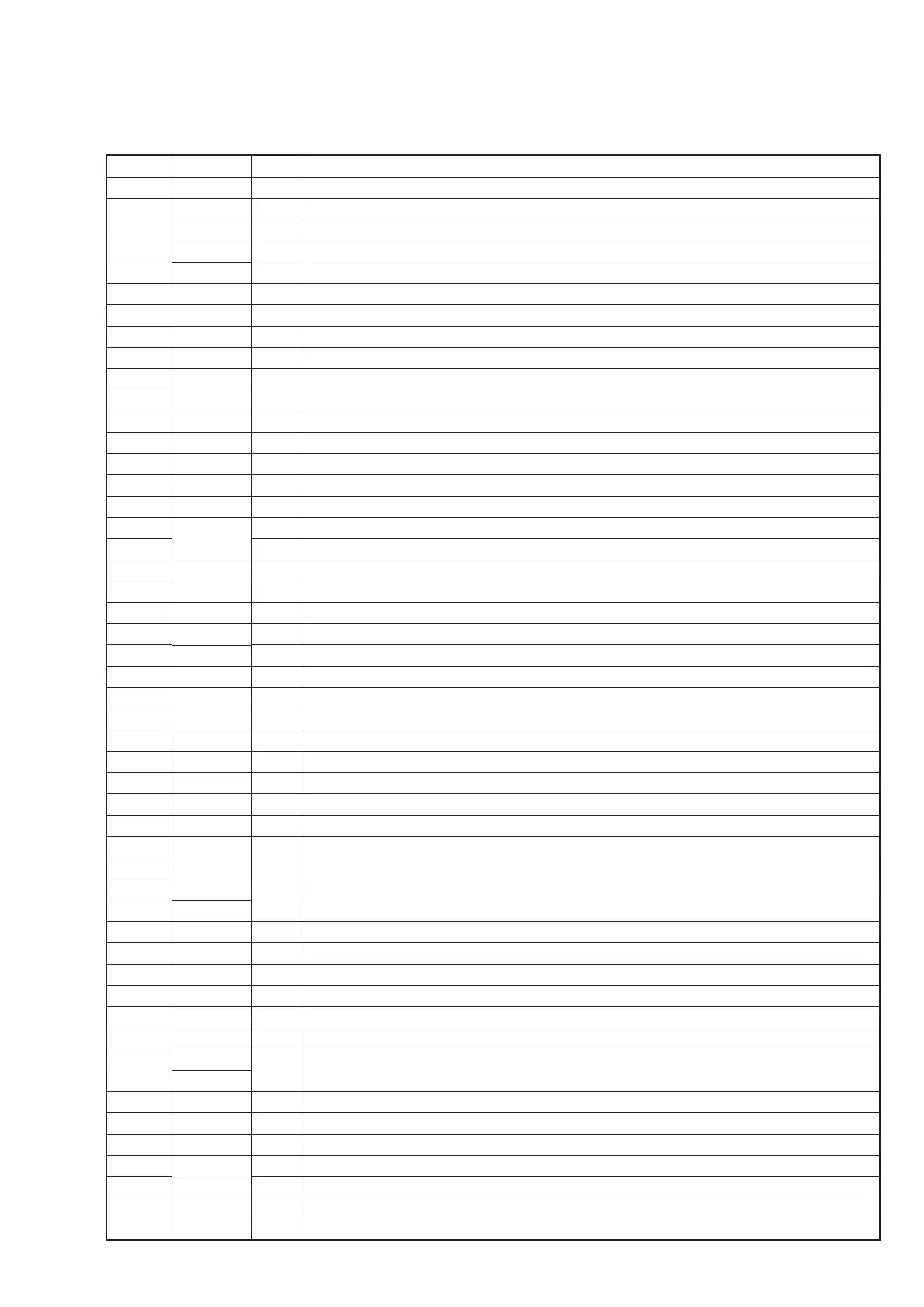
5-1. IC PIN FUNCTION DESCRIPTION
Pin No.
1
2
3
4
5
6
7
8
9
10
11
12
13
14
15
16
17
18
19
20
21
22
23
24
25
26
27
28
29
30
31
32
33
34
35
36
37
38
39
40
41
42
43
44
45
46
47
48
49
50
—
68
I/O
—
I/O
I
O
O
O
O
O
O
O
I
O
O
I
I
I
I
I
I
I
I
—
—
—
I
I
I
O
O
O
I
O
O
O
I
I
I/O
I
I
I
I
O
O
O
O
O
O
O
—
—
Pin Name
VSS
NC
FOK_1
AGCPWM_O
NC
NC
AMUTE_O
VCC2ON_O
XRST_O
SCK_O
MSDTI_I
MSDTO_O
WAKEUP_O
AD_SEL
AD_CHGMNT
AD_KEY2
AD_BATMNT
AD_KEY
AD_RMKEY
AD_DCINMNT
WP_OPEN
VREFL
VREFH
VDD
SCOR_I
GRSCOR_I
SPDL-MTR/FG_I
BEEP_O
NC
RMSCK_O
RMDATI_I
RMDATO_O
RMRW_O
RMRAT_O
WFCK_I
COMPON_I
SLVCD_I
AVLS_I
HOLD_I
BATDET_I
DSP_SEL_I
XHGON_I
XLAT_O
XSOE_O
VOL_LT_O
XPOWLT_O
XDOUTON_O
XAPC_OFF_O
NC
SEG14
—
0
Description
Digital GND
—
FOK input
AGC PWM control (f=7.8kHz)
XWRE monitor (for debug purpose on)
XQOK monitor (for debug purpose on)
Analog mute on
VCC2 switching
System reset
Serial clock to CXD3027R
Serial input from CXD3027R
Serial output to CXD3027R
CXD3027R wake up
Mode selection
Charging monitor
Set key detection
Battery monitor
Lid key detection
Remocon key detection
DC-in monitor
Lid-open detection
Analog GND for A/D
Analog Vdd for A/D
Digital Vcpu
SCOR input
GRSCOR input
WFCK input
BEEP sound (2.06kHz, 50% duty)
—
Serial clock to CXD751
Serial input from CXD751
Serial output to CXD751
CXD751 readwrite selection
CXD751 serial data latch
—
G-protection selection
—
AVLS selection
HOLD selection
Bottom cell detection
“H”: CXD3027R, “L”: CXD3037R
Pick-up Vcc control
CXD3027R serial data latch
CXD3027R serial data output enable
Analog switch on when L/O inserted
TB2119F serial data latch
Digital out LED control
APC mute
—
LCD segment output
• IC801 TMP88CM22F (MICRO COMPUTER)
SECTION 5
DIAGRAMS