77
DR-BT21G
DR-BT21G
SECTION 3
DIAGRAMS
For schematic diagrams.
Note:
• All capacitors are in µF unless otherwise noted. (p: pF)
50 WV or less are not indicated except for electrolytics
and tantalums.
• All resistors are in Ω and
1
/
4
W or less unless otherwise
specified.
•%: indicates tolerance.
• C : panel designation.
• A : B+ Line.
• Power voltage are dc 3.7 V and fed with regulated dc
power supply from battery terminal.
•Voltages are dc with respect to ground under tolerances.
no mark : STANDBY
(): AC ADAPTOR IN
•Voltages are taken with a VOM (Input impedance 10 MΩ).
Voltage variations may be noted due to normal produc-
tion tolerances.
• Signal path.
F : AUDIO
NOTE FOR PRINTED WIRING BOARDS AND SCHEMATIC DIAGRAMS.
Caution:
Parts face side: Parts on the parts face side seen from
(Side A) the parts face are indicated.
Pattern face side: Parts on the pattern face side seen from
(Side B) the pattern face are indicated.
For printed wiring boards.
Note:
• X : parts extracted from the component side.
• Y : parts extracted from the conductor side.
•
: Pattern from the side which enables seeing.
(The other layers' patterns are not indicated.)
• IC101 (CXN1450-2ABL) on MAIN board cannot be replaced
individually.
Replace it with “MAIN BOARD, COMPLETE”.
• The voltage of IC101 cannot be measured.
• MAIN board is four-layer pritnted board.However, the patterns of
layer 2 and 3 have not been included in this diagrams.
OUT
BAT
VCC
ISET
IN
VCC VCC
VCC
STAT2
VSS
9
10
8
7
6
2
3
5
1
4
I
(DETECT)
ENABLE
V
(ISET)
V
I(BAT)
V
I(BAT)
V
I(BAT)
V
I(BAT)
V
(RCH)
V
(PRECHG)
V
(TAPER)
V
(TERM)
VSET
V
I(BAT)
V
I(SET)
V
I(SET)
V
(SLP)
V
O(REG)
V
O(REG)
V
O(REG)
VSET
CHG ENABLE
CHG ENABLE
CHG ENABLE
I
(FAULT)
ENABLE
I
(DETECT)
ENABLE
I
(FAULT)
ENABLE
DEGLITCH
DEGLITCH
DEGLITCH
DEGLITCH
RECHARGE
PRECHARGE
TAPER
TERM
STAT1
REFERENCE
AND BIAS
THERMAL
SHUTDOWN
CHARGE
CONTROL,
TIMER,
AND
DISPLAY
LOGIC
PG
PG
TS
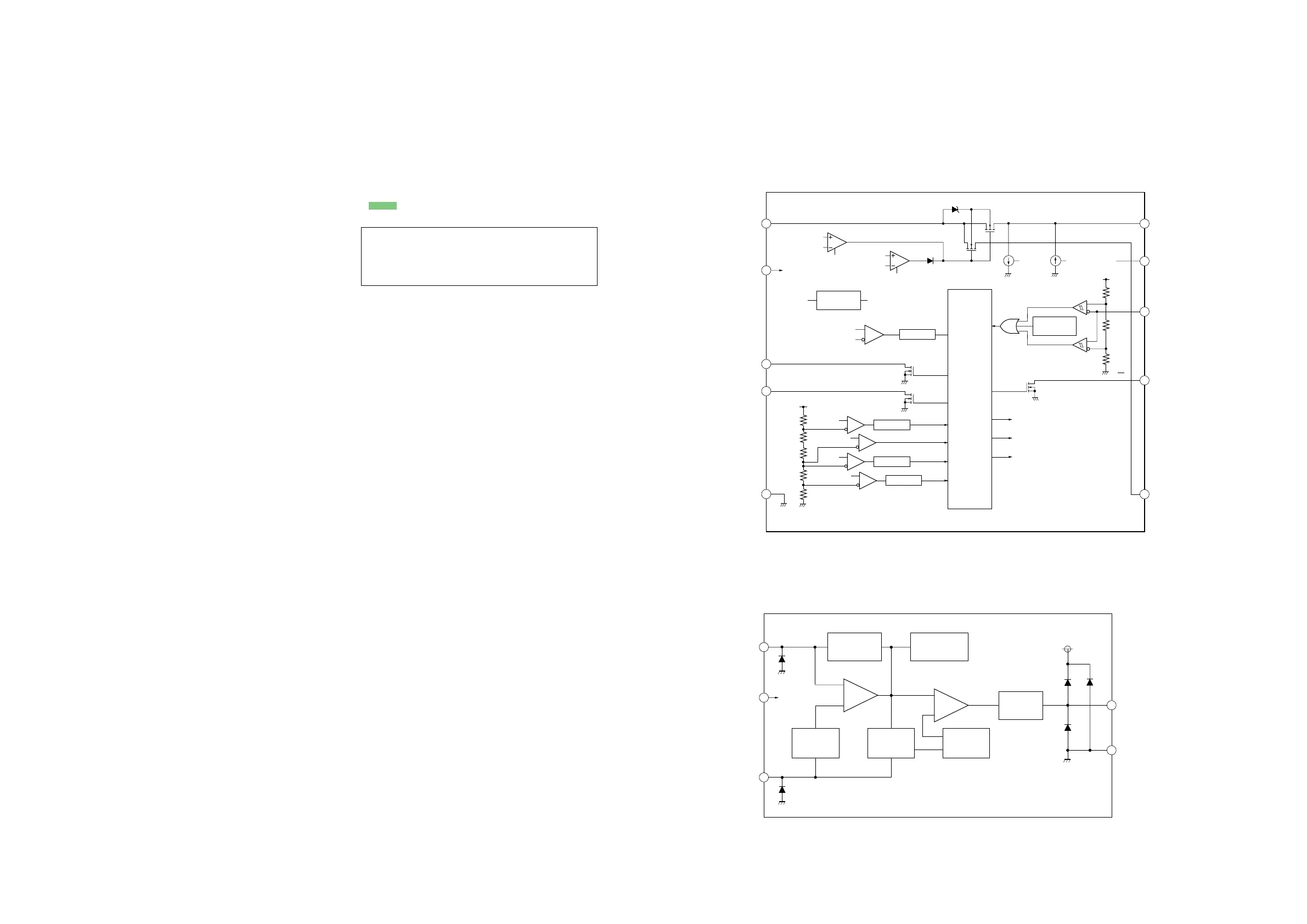
IC261 BQ24010ADRCR
• IC Block Diagram
- CHARGER Board -
IC251 XC9103D093MR
1FB
VDD VDD
VDD
2
CE
3
EXT
5
4 GND
–
+
–
+
VREF WITH
SOFT START,
CE
PWM/PFM
CONTROLER
RAMP WAVE
GENERATOR,
OSC
BAFFER,
DRIVER
PWM
COMPARATOR
ERROR AMP
CURRENT
RIPPLE DETECT
AND FB
PHASE
COMPENSATION


 To Next Page