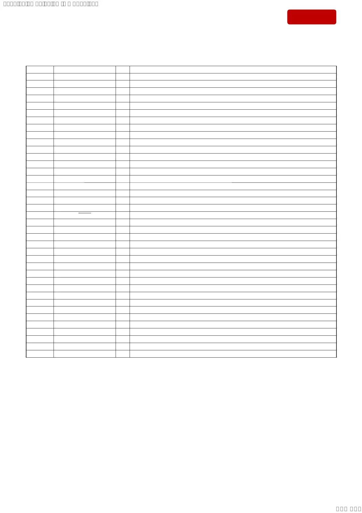
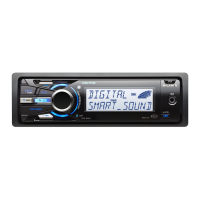
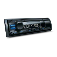
DSX-B700/B700W/B710D
41
Sony CONFIDENTIAL
For Authorized Servicer
• IC Pin Function Description
MAIN BOARD IC101 MAX2172ETL+T (DAB RECEIVER)
Pin No. Pin Name I/O Description
1 VTUNE I High-impedance VCO tune input terminal
2 VCC_LDO - Power supply terminal (+3.3V)
3 LDO_BYPASS - LDO bypass terminal (External capacitor connection terminal)
4 VCC_LBAND - Power supply terminal (+3.3V)
5 NC - Not used
6 LBAND_IN I RF signal input terminal for L-band Not used
7 GND - Ground terminal
8 ADDR I Device address setting terminal Fixed at “L” in this unit
9 VHF_IN I RF signal input terminal for DAB
10, 11 IND1, IND2 - Filter inductor connection terminal
12 AC_GND - AC ground terminal (External capacitor connection terminal)
13 GND - Ground terminal
14 VCC_VHF - Power supply terminal (+3.3V)
15 AC_GND - AC ground terminal (External capacitor connection terminal)
16 VCC_MIX - Power supply terminal (+3.3V)
17 VCC_BB - Power supply terminal (+3.3V)
18 GND - Ground terminal
19 RFAGC I Gain control input terminal (External capacitor connection terminal)
20 RSSI_DELAY O Relative signal strength inductor output terminal (External capacitor connection terminal)
21 STBY
I Standby enable signal input from the DAB audio DSP “L”: standby
22 BBOUT– O Audio signal (negative) output to the DAB audio DSP
23 BBOUT+ O Audio signal (positive) output to the DAB audio DSP
24 QDC+ - Q-channel DC offset bypass terminal for connect to the QDC– (pin 25)
25 QDC– - Q-channel DC offset bypass terminal for connect to the QDC+ (pin 24)
26 BBAGC I Gain control signal input from the DAB audio DSP
27 IDC+ - I-channel DC offset bypass terminal for connect to the IDC– (pin 28)
28 IDC– - I-channel DC offset bypass terminal for connect to the IDC+ (pin 27)
29 MUX O Multiplex output terminal Not used
30 REF_OUT O Reference clock output to the DAB audio DSP
31 VCC_XTAL - Power supply terminal (+3.3V)
32 GND - Ground terminal
33 XTAL I System clock input terminal (24.576 MHz)
34 SCL I Serial data transfer clock signal input from the DAB audio DSP
35 SDA I Serial data input from the DAB audio DSP
36 GND - Ground terminal
37 VCC_SYN - Power supply terminal (+3.3V)
38 GND - Ground terminal
39 CPOUT O Charge pump output terminal for the VTUNE (pin 1)
40 GND - Ground terminal
SYSSET
2019/10/2421:43:03(GMT+09:00)