DSX-B700/B700W/B710D
42
Sony CONFIDENTIAL
For Authorized Servicer
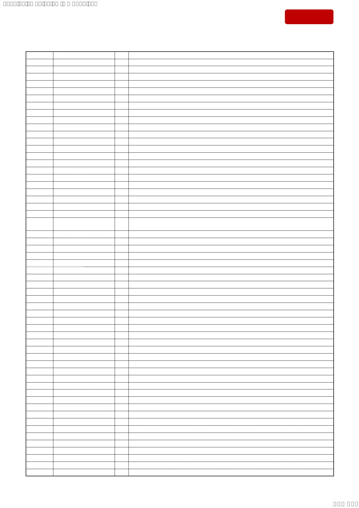
MAIN BOARD IC102 FS1235-A (A/D CONVERTER, DAB AUDIO DSP)
Pin No. Pin Name I/O Description
1 LDO3V3 - Power supply terminal (+3.3V) (for LDO)
2 VDDIORF - Power supply terminal (+3.3V)
3 SDA0 O Serial data output to the DAB receiver
4 SCL0 O Serial data transfer clock signal output to the DAB receiver
5 XTI I Reference clock input from the DAB receiver and XTO (pin 6)
6 XTO O Reference clock output to the XTI (pin 5)
7 PDM0 O Gain control signal output to the DAB receiver
8 PDM1 I/O Not used
9 AVDDCOREPLL - Power supply terminal (+1.2V) (for PLL)
10 AVSSCOREADC - Ground terminal (for ADC)
11 AVDDCOREADC - Power supply terminal (+1.2V) (for ADC)
12 RFIQB I RF signal (negative) input terminal Fixed at “L” in this unit
13 RFIQ I RF signal (positive) input terminal Fixed at “L” in this unit
14 RFII I Audio signal (positive) input from the DAB receiver
15 RFIIB I Audio signal (negative) input from the DAB receiver
16 AVDDIOANA O Power supply output terminal (+2.5V) (for analog)
17, 18 RFIVIN1, RFIVIN0 I Audio signal input terminal Not used
19 VDDCORE_0 - Power supply terminal (+1.2V)
20 VDDIODIG1_0 - Power supply terminal (+3.3V)
21 RFIPWRD_N O Standby enable signal output to the DAB receiver “L”: standby
22, 23 GPIO_0, GPIO_3 I/O Not used
24 SDA1 I/O Two-way IIC data bus with the system controller
25 to 27
GPIO_1, GPIO_2,
GPIO_4
I/O Not used
28 VDDCORE_1 - Power supply terminal (+1.2V)
29 SCL1 I IIC clock signal input from the system controller
30 GPIO_5 I/O Not used
31 SCL2 I/O Two-way serial clock signal terminal Not used
32 SDA2 I/O Two-way serial data bus terminal Not used
33 SOUT O UART serial data output terminal Not used
34 SIN I UART serial data input terminal Not used
35 GPIO_6 I/O Not used
36 CS1_N_2 O Chip select signal output to the serial fl ash
37 SPD_OUT O SPDIF signal output terminal Not used
38 VDDIODIG1_1 - Power supply terminal (+3.3V)
39 POR_N I DAB power supply on/off control signal input from the system controller “H”: power on
40 CS1_N_0 O Chip select signal output to the serial fl ash
41 VDDCORE_2 - Power supply terminal (+1.2V)
42 TXD1 O Serial data output to the serial fl ash
43 RXD1 I Serial data input from the serial fl ash
44 VDDIODIG2_0 - Power supply terminal (+3.3V)
45 SCLKO1 O Serial data transfer clock signal output to the serial fl ash
46 DACLK O Audio clock signal output terminal Not used
47 WS I/O Two-way frame clock signal with the FM/AM receiver
48 BCLK I/O Two-way bit shift clock signal with the FM/AM receiver
49 SDO_0 O Audio data output to the FM/AM receiver
50 TDI I Test data input terminal Not used
51 TCK I Test clock input terminal Not used
52 TDO O Test data output terminal Not used
53 TMS I Test mode selection signal input terminal Not used
54 PDM2 I/O Not used
55 CS1_N_1 O Chip select signal output terminal Not used
56 VDDCORE_3 - Power supply terminal (+1.2V)
57 VDDIODIG1_2 - Power supply terminal (+3.3V)
58 AVDDIOUSB - Power supply terminal (+3.3V)
59 AVSSIOUSB - Ground terminal
60 USB_RREFEXT I/O External bias resistor connection terminal
61 USBP I/O Two-way USB data (positive) bus terminal Not used
SYSSET
2019/10/2421:43:03(GMT+09:00)